
Manufacturing method of fin field-effect transistor

A technology of fin field effect and manufacturing method, which is applied in semiconductor/solid-state device manufacturing, semiconductor devices, electrical components, etc., can solve the problem of reducing device stability, uneven surface morphology of shallow trench isolation 11, and oxide surface morphology. Inconsistent appearance and other problems, to achieve the effect of reducing aspect ratio, improving flatness, and improving appearance

Inactive Publication Date: 2015-02-18
SHANGHAI HUALI MICROELECTRONICS CORP
View PDF3 Cites 2 Cited by
  • Summary
  • Abstract
  • Description
  • Claims
  • Application Information

AI Technical Summary

Problems solved by technology

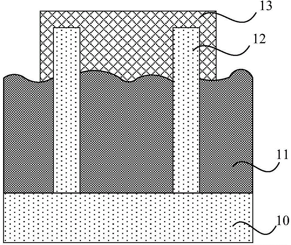
Since the vertical fins of the fin structure 12 are not conducive to the filling of oxide, the surface morphology of the filled oxide is inconsistent, and the etch-back oxide process can easily cause the surface morphology of the formed shallow trench isolation 11 to be uneven.
This will obviously greatly reduce the stability of the device

Method used


Image

  • Manufacturing method of fin field-effect transistor
  • Manufacturing method of fin field-effect transistor
  • Manufacturing method of fin field-effect transistor

Examples


Embodiment Construction

[0028] In order to make the purpose and features of the present invention more obvious and easy to understand, the following will further describe the specific embodiments of the present invention in conjunction with the accompanying drawings. However, the present invention can be realized in different forms, and should not be considered as being limited to the described embodiments .

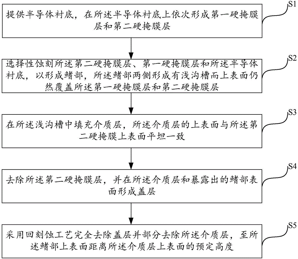
[0029] Please refer to figure 2 , an embodiment of the present invention provides a method for manufacturing a fin field effect transistor, comprising the following steps:

[0030] S1, providing a semiconductor substrate, on which a first hard mask layer and a second hard mask layer are sequentially formed;

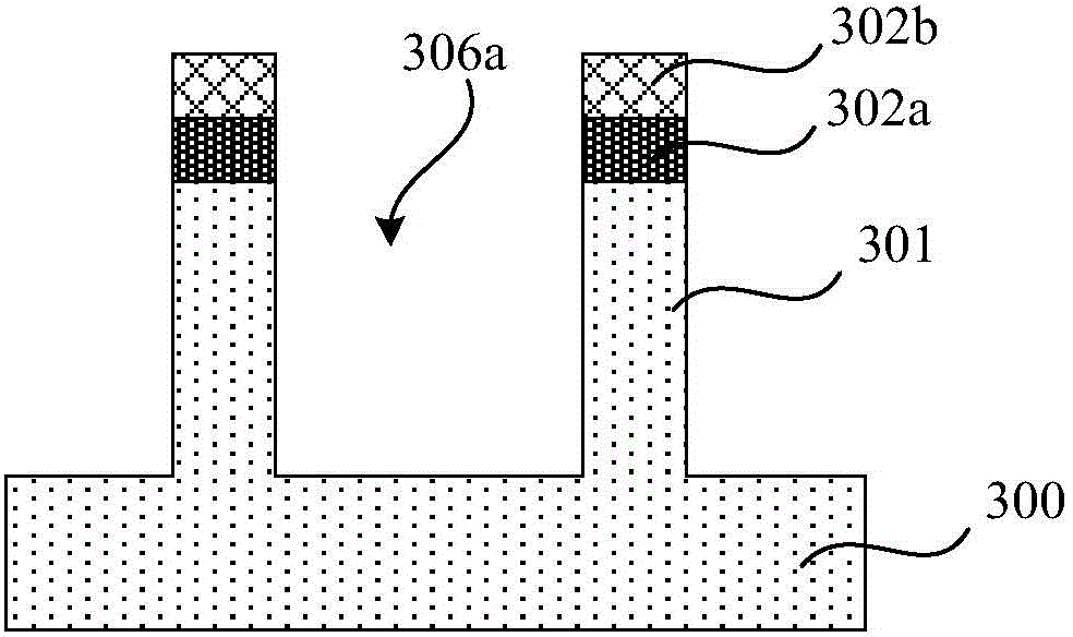
[0031] S2, selectively etching the second hard mask layer, the first hard mask layer and the semiconductor substrate to form fins, shallow trenches are formed on both sides of the fins and the upper surface still covers the The first hard mask layer and the second hard mask layer;

[0...


PUM


Abstract

The invention provides a manufacturing method of a fin field-effect transistor. Before a dielectric layer is etched back to form a shallow trench isolation structure among fins, removing the top one of two hard mask layers pre-formed on the upper surface of each fin, and forming a cover layer on the whole device surface. The cover layer allows shallow trench filler to be wider, the shape of the shallow trench filler is improved, the depth-width ratio of an etch-back window is reduced, and the surface flatness of the etched-back shallow trench isolation structure is improved; the residual hard mask layers keep side structures of the fins exposed, and finally device performance of the fin field-effect transistor is improved.

Description

technical field [0001] The invention relates to the technical field of semiconductor manufacturing, in particular to a method for manufacturing a fin field effect transistor. Background technique [0002] MOS transistors generate switching signals by regulating the current through the channel region by applying a voltage to the gate. However, when the semiconductor technology enters the node below 45 nanometers, the control ability of the traditional planar MOS transistor on the channel current becomes weak, causing serious leakage current. That is, the so-called short-channel effects (SCE: short-channel effects) are more likely to occur. [0003] For this reason, the planar CMOS transistor is gradually transitioning to a three-dimensional (3D) Fin Field Effect Transistor (Fin Field Effect Transistor, FinFET) device structure. In FinFET, the gate can control the ultra-thin body at least from both sides, which has a much stronger gate-to-channel control ability than planar ...

Claims


Application Information

Patent Timeline
IPC IPC(8): H01L21/336
CPCH01L29/66795
Inventor 鲍宇
Owner SHANGHAI HUALI MICROELECTRONICS CORP
Learn More