Making methods and apparatuses of flexible substrate circuit board and metal pinning layer

A technology of flexible substrates and metal nails, applied in the electronic field, can solve the problems of weak anti-peel strength, decreased bonding strength, and insufficient bonding force of the film layer, and achieve the effect of good bonding force and enhanced anti-peeling strength

Active Publication Date: 2015-02-25
BEIJING NORMAL UNIVERSITY
View PDF4 Cites 18 Cited by
  • Summary
  • Abstract
  • Description
  • Claims
  • Application Information

AI Technical Summary

Problems solved by technology

[0004] The base material formed by the adhesive can no longer meet the high-density assembly requirements
And, in the substrate circuit board that existing FPC adopts, when going through follow-up procedures such as circuit pattern forming process or electrolysis process between each film layer (as fil

Method used


Image

  • Making methods and apparatuses of flexible substrate circuit board and metal pinning layer
  • Making methods and apparatuses of flexible substrate circuit board and metal pinning layer
  • Making methods and apparatuses of flexible substrate circuit board and metal pinning layer

Examples


preparation example Construction

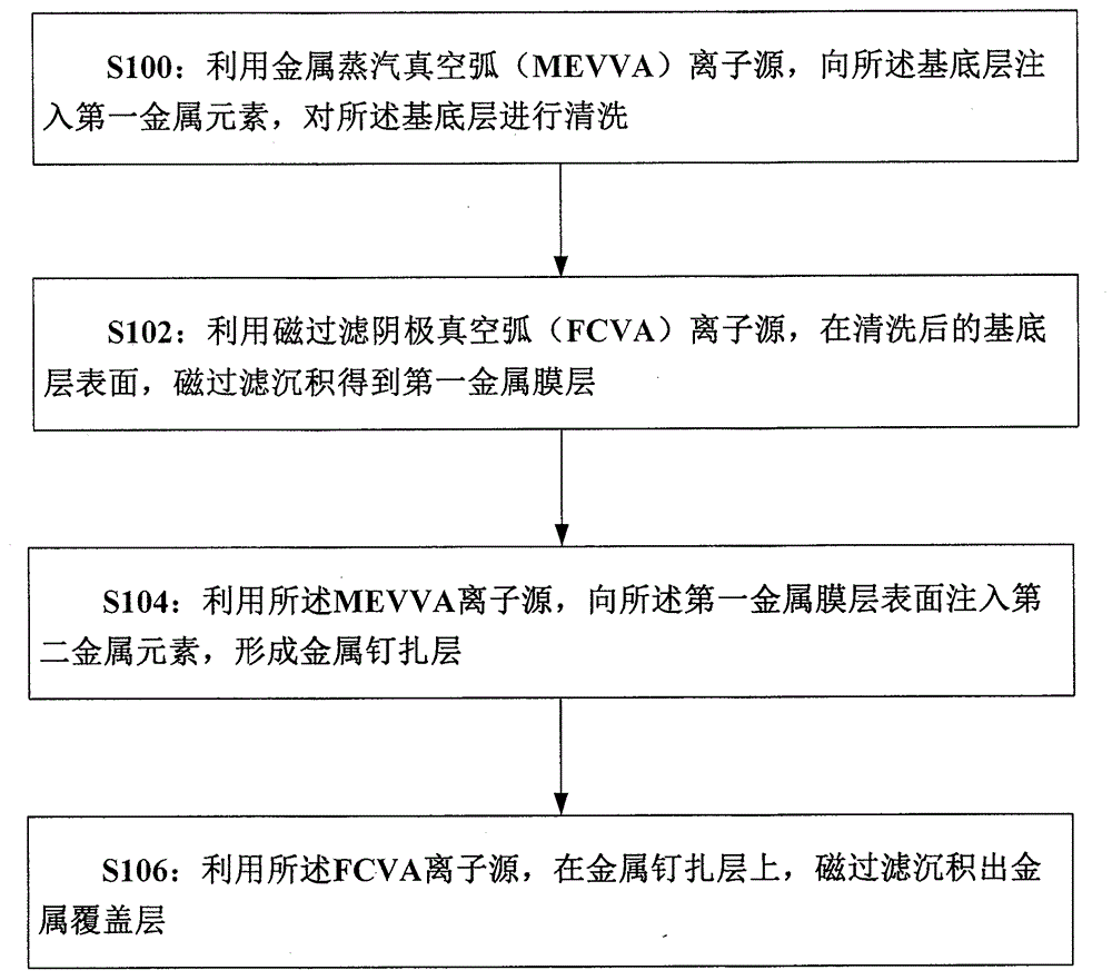
[0047] refer to figure 1 , which shows the preparation method of the metal pinning layer of this embodiment, the preparation method includes the following steps:

[0048]S100: Using a metal vapor vacuum arc (MEVVA) ion source, injecting a first metal element into the base layer to clean the base layer.

[0049] Among them, this step is the cleaning process of metal ion implantation in the early stage. The polyimide film is implanted with high-energy metal ions, which can sputter off the surface to absorb dust and gas, etc., and improve the cleanliness of the surface. In addition, the MEVVA ion source implants metal elements into the polyimide. During the implantation process, the metal elements have certain energy, which can have a certain sputtering effect on the physically adsorbed or chemically adsorbed impurities on the surface of the polyimide film, and can A shallow implanted metal doped layer is formed.

[0050] In addition, before depositing the metal pinning layer, ...

example 1

[0115] Example 1: (no pinning layer structure)

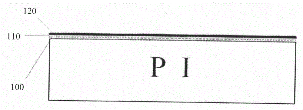
[0116] Using the PI 100HN polyimide film produced by DuPont of the United States as the base material, the polyimide film layer is treated on both sides in the following manner:

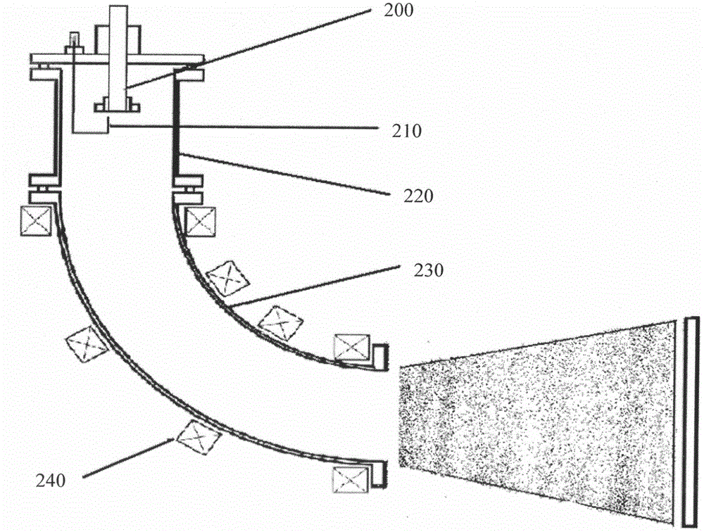
[0117] 1) The Cu film transition layer was deposited by magnetic filtration, the conditional arc current was 100A, the magnetic field current of the elbow was 2.0A, and the deposition thickness was 20nm.

[0118] 2) Electroplating in a copper sulfate solution to form a copper film with a thickness of 20 μm.

example 2

[0119] Example 2: (Cu metal is selected as the structural element of the pinning layer)

[0120] 1) Cleaning: ion implantation of Cu element conditions: implantation high voltage 6kV, implantation beam intensity 3mA, implantation dose 3×10 15 ;

[0121] 2) Magnetic filtration deposition Cu film conditions: arc current 100A, elbow magnetic field current 2.0A, deposition thickness 8nm;

[0122] 3) Perform Cu ion implantation on the Cu thin layer to form a pinning layer Conditions: accelerating voltage 12kV, beam current 5mA, implant dose 3×10 15 / cm 2 ;

[0123] 4) Covering: magnetic filtration deposited Cu film covering layer conditions: arc current 100A, elbow magnetic field current 2.0A, deposition thickness 20nm;

[0124] 5) Finally, electroplating in a copper sulfate solution to form a copper film with a thickness of 20 μm.


PUM

PropertyMeasurementUnit
Thicknessaaaaaaaaaa
Thicknessaaaaaaaaaa

Abstract

The invention discloses making methods and apparatuses of a flexible substrate circuit board and a metal pinning layer. The making method of the metal pinning layer comprises the following steps: injecting a first metal element into a substrate layer by using a metal vapor vacuum arc (MEVVA) ion source, and cleaning the substrate layer; carrying out magnetic filtering deposition on the surface of the cleaned substrate layer by using a magnetic filtered cathodic vacuum arc (FCVA) ion source to obtain a first metal film; and injecting a second metal element to the surface of the first metal film by using the MEVVA ion source to form the metal pinning layer. The metal pinning layer and the flexible substrate circuit board made by adopting the making methods and the apparatuses have very high bonding force and peeling resistance.

Description

technical field [0001] The invention relates to the field of electronic technology, in particular to a method and equipment for preparing a flexible substrate circuit board and a metal pinning layer. Background technique [0002] At first, flexible circuit boards (FPC) were only used in special industries such as military and aerospace, but with the advancement of science and technology and the development of various information terminal equipment, FPC has gradually been applied to civilian and commercial fields. Like rigid circuit boards, FPC achieved great development. However, compared with rigid circuit boards, FPC is smaller in size and lighter in weight, and can realize bending and bending and three-dimensional three-dimensional assembly. [0003] With the continuous advancement of technology, the demand for FPC has also increased. At present, an adhesive is usually used to attach copper foil to a flexible plastic substrate to prepare FPC. However, the inventors of ...

Claims


Application Information

Patent Timeline
IPC IPC(8): C23C14/20C23C14/48C23C14/46
Inventor 廖斌吴先映张旭张荟星陈琳
Owner BEIJING NORMAL UNIVERSITY
Why Eureka
Try Eureka