Quasi molecule laser annealing apparatus and preparation method of low-temperature polysilicon thin film

An excimer laser and annealing device technology, which is applied in semiconductor/solid-state device manufacturing, electrical components, circuits, etc., can solve the problems of lower annealing temperature of amorphous silicon thin film 23, difficulty in forming low-molecular polysilicon, and greater influence of annealing time , to achieve the effect of reducing temperature difference, prolonging annealing time and high mobility

Active Publication Date: 2015-03-04
BOE TECH GRP CO LTD
View PDF5 Cites 11 Cited by
  • Summary
  • Abstract
  • Description
  • Claims
  • Application Information

AI Technical Summary

Problems solved by technology

[0005] However, the annealing time has a great influence on the formation of low-temperature polysilicon with large grains, for example, as figure 1 As shown, the amorphous silicon film 23 has a relatively high temperature (above 1000° C.) under laser irradiation, but the temperature of the substrate 21 to be processed is relatively low (usually room temperature), because the amorphous silicon film 23 and the substrate 21 to be processed direct contact and the temperature difference between the two is large, the heat of the amorphous silicon film 23 is rapidly conducted to the substrate 21 to be processed, and is conducted to the workbench 22 by the substrate 21 to be processed, thereby making the annealing of the amorphous silicon film 23 The temperature decreases rapidly, the effective annealing time becomes shorter, and it is difficult to form low-molecular-weight polysilicon with larger grains

Method used


Image

  • Quasi molecule laser annealing apparatus and preparation method of low-temperature polysilicon thin film
  • Quasi molecule laser annealing apparatus and preparation method of low-temperature polysilicon thin film
  • Quasi molecule laser annealing apparatus and preparation method of low-temperature polysilicon thin film

Examples


Embodiment 1

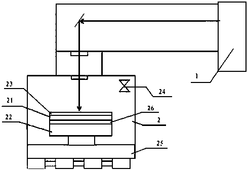
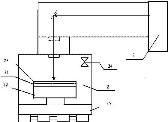
[0027] Such as figure 2 As shown, the present embodiment provides an excimer laser annealing device, comprising: a laser generating unit 1 and a process chamber 2, a workbench 22 is provided in the process chamber 2, and a workbench 22 is provided on the workbench 22 Heating unit 26.

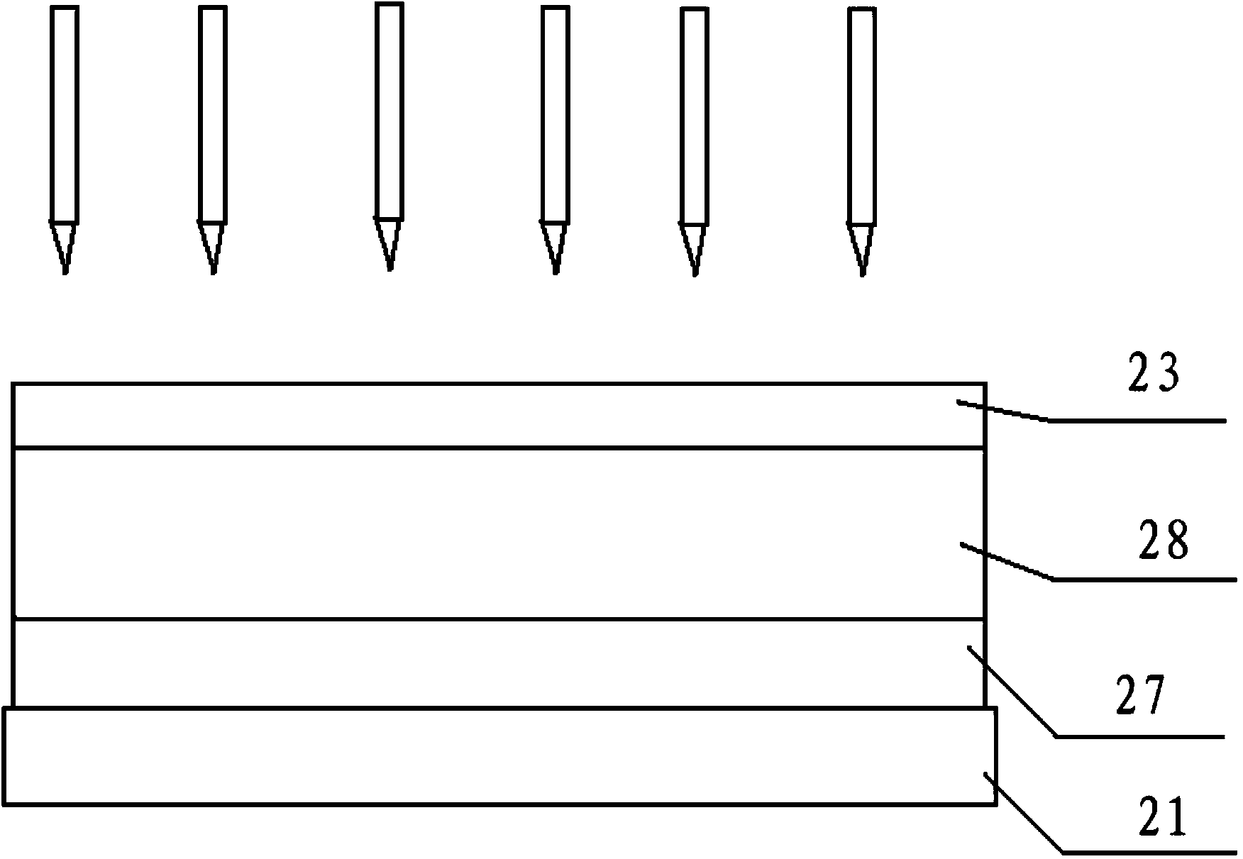
[0028] Such as image 3 As shown, the substrate 21 to be processed includes an amorphous silicon thin film 23 disposed on a buffer layer; the buffer layer includes a silicon nitride layer 27 and a silicon dioxide layer 28 sequentially disposed from the surface of the substrate 21 to be processed.

[0029] When the substrate 21 to be processed is placed on the workbench 22 for annealing, since the workbench 22 is provided with a heating unit 26, the heating unit 26 heats the substrate 21 to be processed during the annealing process of the substrate 21 to be processed, reducing the The temperature difference between the substrate 21 to be processed and the amorphous silicon film 23, laser irrad...

Embodiment 2

[0039] Such as image 3 with figure 2 As shown, this embodiment provides a method for preparing a low-temperature polysilicon thin film, comprising the following steps:

[0040] A thin film of amorphous silicon is formed on the substrate by a deposition method;

[0041] heating the amorphous silicon film;

[0042] Using a heating unit equipped with excimer laser annealing to heat the substrate to a predetermined temperature and keep it warm;

[0043] The amorphous silicon thin film is annealed by an excimer laser annealing device.

[0044] Since the substrate is heated and then the amorphous silicon film is annealed, the heat of the melted amorphous silicon will not be quickly conducted to the substrate, resulting in a rapid drop in the temperature of the melted amorphous silicon, resulting in insufficient annealing time, which cannot A polysilicon film with large grains is formed.

[0045] The above method is easy to operate in the production process, the process is sim...


PUM

PropertyMeasurementUnit
diameteraaaaaaaaaa
diameteraaaaaaaaaa

Abstract

The invention provides a quasi molecule laser annealing apparatus and a preparation method of a low-temperature polysilicon thin film, for solving the problems of short effective annealing time and quite small crystal grains during annealing of a conventional low-temperature polysilicon thin film in the prior art. In the quasi molecule laser annealing apparatus, a heating unit is arranged at one side, which is far away from an amorphous silicon thin film, at a substrate to be processed, for heating the substrate to the processed. The heating unit heats the substrate during the annealing process of the substrate to be processed, such that the temperature difference between the substrate to the processed and the amorphous silicon thin film is reduced, heat generated when laser is irradiated on the amorphous silicon thin film is not rapidly conducted to the substrate, the temperature reduction speed of the amorphous silicon thin film is slowed down, the annealing time is prolonged, and fused amorphous silicon can be conveniently annealed to form the large-crystal-grain polysilicon thin film. Since the preparation method of the low-temperature polysilicon thin film employs the quasi molecule laser annealing apparatus, the large-crystal-grain polysilicon thin film can be obtained, and a polysilicon thin film transistor with higher mobility can be obtained.

Description

technical field [0001] The invention relates to the field of display technology, in particular to an excimer laser annealing device and a method for preparing a low-temperature polysilicon thin film. Background technique [0002] Organic electroluminescent display has become the best choice for future display technology due to its advantages of high image quality, short response time of moving images, low power consumption, wide viewing angle and ultra-light and ultra-thin. At present, in the organic electroluminescent display, the production of the polysilicon layer in the backplane technology can adopt various production methods such as excimer laser annealing, solid-phase crystallization, and metal-induced crystallization. However, using the excimer laser annealing process to prepare the polysilicon thin film of the active layer of the transistor in the backplane is the only method that has achieved mass production. [0003] Such as figure 1 As shown, the excimer laser ...

Claims


Application Information

Patent Timeline
Patent Type & Authority Applications(China)
IPC IPC(8): H01L21/268
CPCH01L21/268H01L21/324H01L21/67115
Inventor 田雪雁
Owner BOE TECH GRP CO LTD
Why Eureka
Try Eureka