Manufacturing method of ultrathin printed circuit board, and ultrathin printed circuit board

A technology of printed circuit board and manufacturing method, applied in the directions of printed circuit manufacturing, printed circuit, printed circuit components, etc., to prevent deformation and avoid scrapping

Active Publication Date: 2015-03-04
SHANGHAI MEADVILLE ELECTRONICS +1
View PDF5 Cites 9 Cited by
  • Summary
  • Abstract
  • Description
  • Claims
  • Application Information

AI Technical Summary

Problems solved by technology

This also brings new challenges to the manu

Method used


Image

  • Manufacturing method of ultrathin printed circuit board, and ultrathin printed circuit board
  • Manufacturing method of ultrathin printed circuit board, and ultrathin printed circuit board
  • Manufacturing method of ultrathin printed circuit board, and ultrathin printed circuit board

Examples


Embodiment 1

[0054] The method for making an ultra-thin printed circuit board is characterized in that it comprises the following steps:

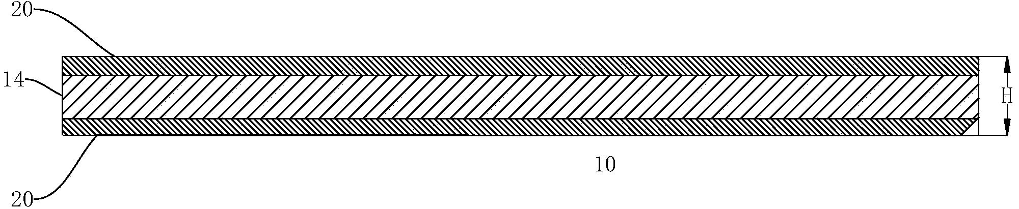
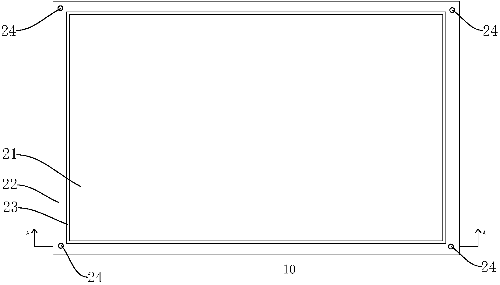
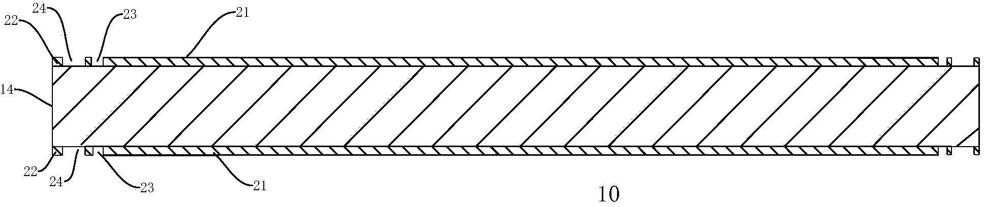
[0055] a. If figure 1 As shown, a polymer material core board 14 is provided, and a positioning copper foil 20 is respectively arranged on the upper surface and the lower surface, and the positioning copper foil 20 is bonded to the polymer material core board 14 . Such as figure 2 , image 3 As shown, pattern transfer, etching or milling is performed on the positioning copper foil 20 to form a through groove 23 so that the positioning copper foil 20 forms a positioning template 21 and a positioning frame 22 . The positioning frame 22 surrounds the positioning template 21 . A positioning pattern 24 is formed on the positioning frame 22 . The positioning figure 24 is formed by removing a part or all of the positioning frame 22 along the thickness direction, or removing a part or all of the other positioning frames except the positioning figure 24 alo...

Embodiment 2

[0067] Such as Figure 11 As shown, this embodiment is based on Embodiment 1. In step e, after the second copper foil 6 located on the outermost side is processed into the second conductive circuit 61, the surface of the second conductive circuit 61 is covered with the second adhesive. junction sheet 81 and third copper foil 82 . The second bonding sheet 81 covers the second conductive circuit 61 . The position of the third copper foil 82 is determined by using the infrared positioning edge. After lamination, the third copper foil 82 is electrically connected to one or both of the second conductive circuit 61 and the first copper foil 4 by drilling and electroplating according to the position of the positioning through hole 13 . Such as Figure 12 As shown, according to the position of the positioning through hole 13, the pattern transfer process is performed on the third copper foil 82 to form the third conductive line 83.

[0068] In step f, the mechanical milling cutter...

Embodiment 3

[0071]On the basis of Embodiment 2, in step e, after processing the outermost third copper foil 82 into a third conductive circuit 83 , the surface of the third conductive circuit 83 is covered with the third bonding sheet 91 and the fourth copper foil. The third bonding sheet 91 covers the third conductive circuit 83 . After lamination, according to the position of the positioning through hole 13, drilling, electroplating, so that the fourth copper foil and one or both of the third conductive circuit 83, the second conductive circuit 61 and the first copper foil 4 are electrically connected. connect. According to the positions of the positioning through holes 13 , the pattern transfer process is performed on the fourth copper foil to form the fourth conductive lines 93 .

[0072] In step f, the mechanical milling cutter longitudinally cuts the product obtained in step e. According to the position of the positioning through hole 13 , it is determined that the cutting path do...


PUM

PropertyMeasurementUnit
Thicknessaaaaaaaaaa
Thicknessaaaaaaaaaa

Abstract

The invention discloses a manufacturing method of an ultrathin printed circuit board, and an ultrathin printed circuit board. According to the manufacturing method, copper foils and bonding plates are laminated at a support plate in hot-pressing mode and the thin copper foils and the thin bonding plates are supported by the support plate. Therefore, plate thickness limitation by equipment in production of electroplating and graph transferring and the like can be effectively eliminated; deformation like warping, bending, and small wrinkle existence and the like of carriers including a first copper foil, a second copper foil and a conductive layer and the like during the lamination and hot pressing process can be effectively improved; and problems of scrapping of the printed circuit board and low yield of the board due to insufficient hardness and poor smoothness of the laminated object can be solved.

Description

technical field [0001] The invention relates to the field of circuit board manufacture, in particular to a method for manufacturing an ultra-thin printed circuit board and the ultra-thin printed circuit board. Background technique [0002] Printed Circuit Board (PCB), also known as printed circuit board, is one of the important components of electronic products. Due to the repeatability (reproducibility) and consistency of the pattern of the printed circuit board, the errors of wiring and assembly are reduced, and the maintenance, debugging and inspection time of the equipment are saved. The design can be standardized, which is conducive to interchange; the printed circuit board has high wiring density, small size, and light weight, which is conducive to the miniaturization of electronic equipment; it is conducive to mechanized and automated production, which improves labor productivity and reduces the cost of electronic equipment. [0003] In recent years, circuit boards h...

Claims


Application Information

Patent Timeline
IPC IPC(8): H05K3/46H05K1/02
CPCH05K1/0298H05K3/28H05K3/4635H05K2203/06H05K2203/15
Inventor 韩春华黄伟叶晓青陈晓峰罗永红
Owner SHANGHAI MEADVILLE ELECTRONICS
Why Eureka
Try Eureka