TiO2-quantum-dot-and-MoS2-nanometer-flower-combined heterojunction semiconductor material and preparation method thereof

A nanoflower and heterojunction technology, applied in nanotechnology, nanotechnology, chemical instruments and methods, etc., can solve the problems of inappropriate large-scale industrial production, complex synthesis process, high production cost, etc. High repeatability, reduced complexity effects

Inactive Publication Date: 2015-03-11
EAST CHINA NORMAL UNIV
View PDF3 Cites 27 Cited by
  • Summary
  • Abstract
  • Description
  • Claims
  • Application Information

AI Technical Summary

Problems solved by technology

[0003] Recently, the academic community has begun to try the combination of two semiconductor materials, and has achieved remarkable results in photocatalysis and lithium-ion batteries. However, m...

Method used


Image

  • TiO2-quantum-dot-and-MoS2-nanometer-flower-combined heterojunction semiconductor material and preparation method thereof
  • TiO2-quantum-dot-and-MoS2-nanometer-flower-combined heterojunction semiconductor material and preparation method thereof
  • TiO2-quantum-dot-and-MoS2-nanometer-flower-combined heterojunction semiconductor material and preparation method thereof

Examples


Embodiment 1

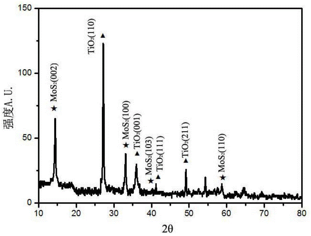
[0037] Embodiment 1 prepares TiO 2 Quantum dot composite MoS 2 Nanoflower Heterojunction Semiconductor Materials

[0038] The specific steps of preparation are as follows:

[0039] (1) Dissolve 1g of sodium molybdate, 1.4g of thiourea and 1.4g of thiourea into 80mL of deionized water, add about 0.33g of oxalic acid to make the pH of the solution less than 1, and stir thoroughly.

[0040] (2) After stirring for more than 15 minutes, add the mixed solution into a 100mL reaction kettle, seal it, then put it into a vacuum oven and heat it at 200°C for 24 hours, and cool to room temperature after the reaction.

[0041] (3) Collect and remove the black precipitate at the bottom of the reaction kettle and the black adhesion on the inner wall, and wash it repeatedly with deionized water until the supernatant is completely clear.

[0042] (4) Pour off the supernatant, put the pure sample in a vacuum oven at 50° C. for 6 hours and take it out after drying to obtain a black powder.

...

Embodiment 2

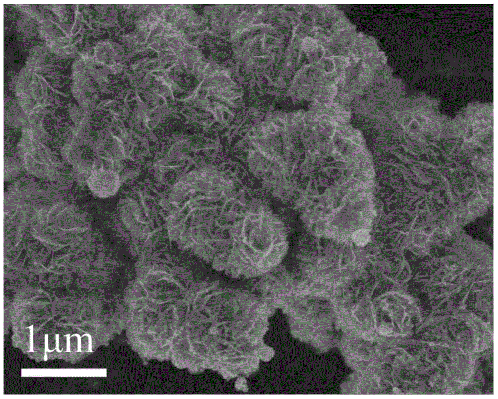
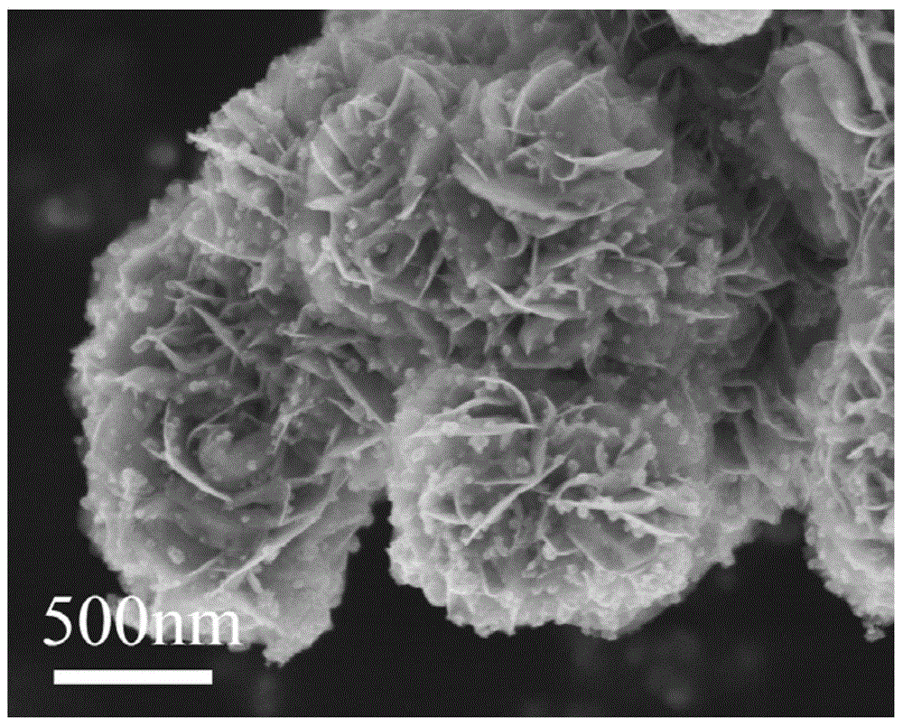
[0048] Embodiment 2 The present invention wave TiO 2 Quantum dot composite MoS 2 Field Emission Performance Test of Nanosphere Composite Heterojunction Semiconductor Materials

[0049] The TiO of the present invention that above-mentioned embodiment 1 prepares 2 Quantum dot composite MoS 2 Nanoflower heterojunction semiconductor material, due to its large specific surface area, forms a p-n junction at the junction, and the distribution of a large number of quantum dots is conducive to electron excitation, making it more effective than pure MoS 2 The photocatalytic performance of nanoflowers has been significantly improved. TiO of the present invention 2 Quantum dot composite MoS 2 Nanoflower heterojunction semiconductor materials and MoS 2 Field emission performance test of nanoflowers, including specific steps:

[0050] (1) get TiO of the present invention respectively 2 Quantum dot composite MoS 2 Nanoflower heterojunction semiconductor materials and pure MoS 2 Add...


PUM


Abstract

The invention discloses a TiO2-quantum-dot-and-MoS2-nanometer-flower-combined heterojunction semiconductor material comprising MoS2 nanometer flower and TiO2 nanometer particles. A large amount of the TiO2 nanometer particles are uniformly distributed on the surface of the MoS2 nanometer flower, and are well compounded on the pedals. The TiO2 nanometer particle phase is in a punctiform dense distribution. The invention also discloses a preparation method of the TiO2-quantum-dot-and-MoS2-nanometer-flower-combined heterojunction semiconductor material. According to the method, with a two-step solvothermal method, the punctiform TiO2 nanometer particles are uniformly grown on the MoS2 nanometer flower, such that the material with a good composite morphology is obtained. The method provided by the invention has the advantages of simple operation, high yield, low preparation cost, and the like. The material provided by the invention has great development and application potential in the fields of photo-catalysis industrial wastewater and field emission.

Description

technical field [0001] The invention belongs to the technical field of optoelectronic materials, semiconductor materials and devices, and specifically relates to a TiO 2 Quantum dot composite MoS 2 Nanoflower heterojunction semiconductor material and its preparation method. Background technique [0002] MoS 2 It is a metal sulfide with a narrow band gap, and it is also a typical two-dimensional layered semiconductor material. The layers are combined by weak van der Waals forces, making MoS 2 It has a wide range of applications in lithium-ion batteries, photocatalysis, field emission and sensors. Rutile TiO 2 It is a metal oxide with a wide bandgap. It is a three-dimensional semiconductor material that is easy to prepare and structurally modified. The granular semiconductor morphology is often used for semiconductor recombination. It is an excellent electron emission shape. [0003] Recently, the academic community has begun to try the combination of two semiconductor m...

Claims


Application Information

Patent Timeline
IPC IPC(8): C01G39/06C01G23/053B82Y30/00B01J27/051
Inventor 郁可傅豪朱自强
Owner EAST CHINA NORMAL UNIV
Why Eureka
Try Eureka