
Electrochromic device and preparation method and application thereof

An electrochromic device and electrochromic layer technology, which can be used in instruments, nonlinear optics, optics, etc., can solve the problems of high production cost and difficulty in large-scale production, and achieve low cost and relatively high production cost. High, easy to achieve results

Inactive Publication Date: 2015-03-11
NINGBO INST OF MATERIALS TECH & ENG CHINESE ACADEMY OF SCI +1
View PDF10 Cites 33 Cited by
  • Summary
  • Abstract
  • Description
  • Claims
  • Application Information

AI Technical Summary

Problems solved by technology

[0004] Based on this, it is necessary to provide an electrochromic device and its preparation method and application in view of the problems that the existing electrochromic devices have high manufacturing costs and are difficult to achieve large-scale production

Method used


Image

  • Electrochromic device and preparation method and application thereof
  • Electrochromic device and preparation method and application thereof
  • Electrochromic device and preparation method and application thereof

Examples


preparation example Construction

[0034] As a specific embodiment of the preparation method of the electrochromic device provided by the present invention, it includes the following steps:

[0035] Step S100, depositing a first conductive layer on the surface of the first substrate by using a coating process.

[0036] Step S200, depositing a first electrochromic layer on the surface of the first conductive layer with a mask.

[0037] In step S300, an electrolyte layer and a second conductive layer are sequentially deposited on the surface of the first electrochromic layer by using a coating process. That is, after the electrolyte layer is deposited on the surface of the first electrochromic layer, the second conductive layer is deposited on the surface of the electrolyte layer. The preparation of the single-layer electrochromic device can be completed. Alternatively, after depositing the second conductive layer on the surface of the second substrate, the second conductive layer and the first electrochromic l...

Embodiment 1

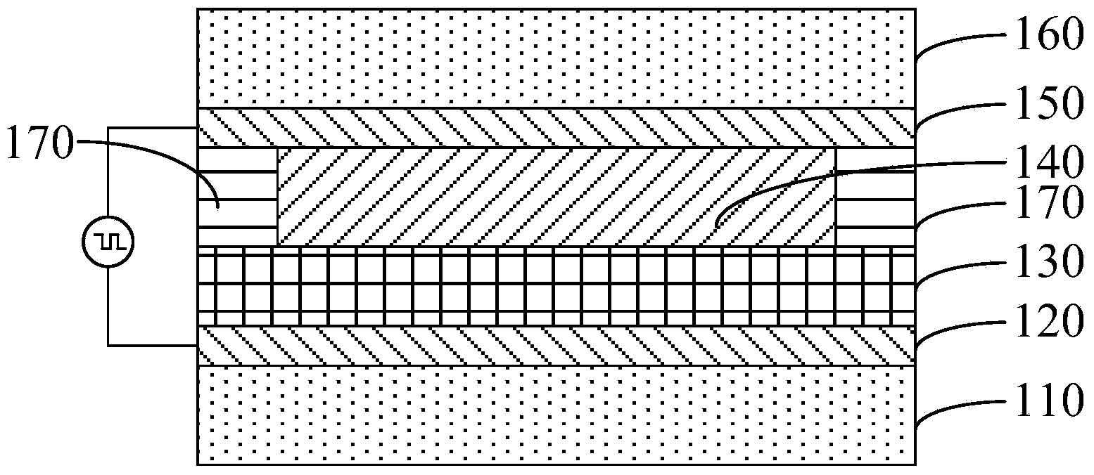
[0066] see figure 1 In the single-layer multi-color electrochromic device provided in Embodiment 1, the first substrate 110 is an ordinary transparent glass sheet. The first conductive layer 120 is an indium tin oxide (ITO) film, which is used to communicate with an external power source and serves as a cathode electrode. The first electrochromic layer 130 is a molybdenum-doped vanadium pentoxide film. The electrolyte layer 140 is a polymer lithium salt solid electrolyte membrane. The second substrate 160 is an ordinary transparent glass sheet. The second conductive layer 150 is an ITO film, which is used to communicate with an external power source and serves as an anode electrode. Use epoxy resin 170 to laminate and seal the two coated transparent glass sheets.

[0067] The preparation method of the above-mentioned single-layer electrochromic device comprises the following steps:

[0068] First, the area cleaned by ultrasonic cleaning with acetone and absolute ethanol s...

Embodiment 2

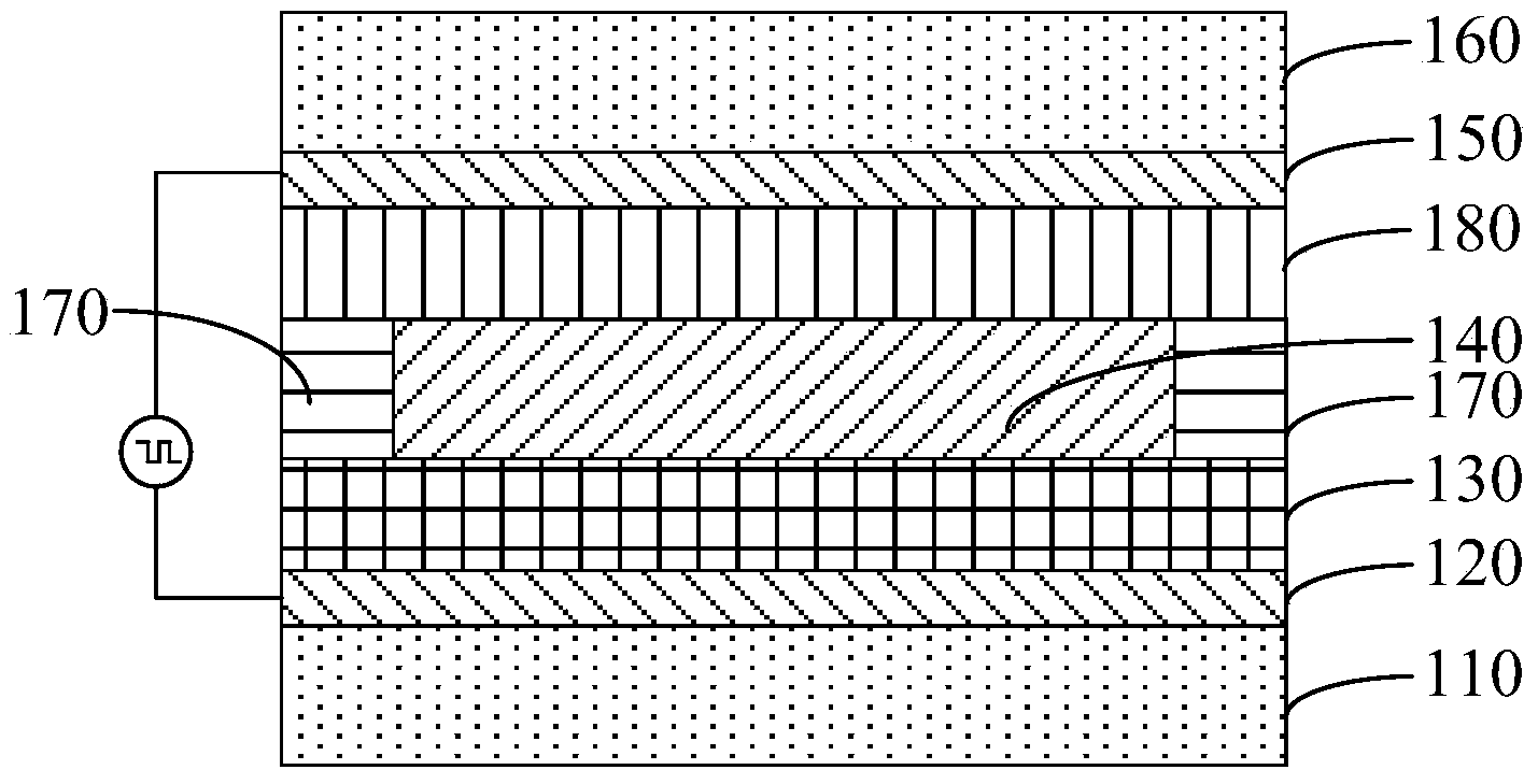
[0078] see figure 2 , is a specific embodiment of a double-layer electrochromic device, and the first substrate 110 is an ordinary transparent glass sheet. The first conductive layer 120 is an indium tin oxide (ITO) film, which is used to communicate with an external power source and serves as a cathode electrode. The first electrochromic layer 130 is a molybdenum-doped vanadium pentoxide film. The electrolyte layer 140 is a polymer lithium salt solid electrolyte membrane. The second substrate 160 is an ordinary transparent glass sheet. The second conductive layer 150 is an indium tin oxide (ITO) film, which is used to communicate with an external power source and serves as an anode electrode. The second electrochromic layer 180 is tungsten oxide (WO 3 ) or nickel oxide (NiO) films. Use epoxy resin 170 to laminate and seal the two coated transparent glass sheets.

[0079] The manufacturing method of the above-mentioned double-layer electrochromic device comprises the fo...


PUM

PropertyMeasurementUnit
Thicknessaaaaaaaaaa
Conductivityaaaaaaaaaa

Abstract

The invention discloses an electrochromic device and a preparation method and application thereof. The preparation method comprises the following steps: depositing a first conductive layer on the surface of a first substrate by adopting a coating process; depositing a first electrochromic layer on a mask on the surface of the first conductive layer; sequentially depositing an electrolyte layer and a second conductive layer on the surface of the first electrochromic layer by adopting a coating process; or preparing an electrolyte layer between the second conductive layer and the first electrochromic layer after the second conductive layer is deposited on the surface of a second substrate; obtaining a single-layer electrochromic device; or, sequentially depositing an electrolyte layer, a second electrochromic layer and a second conductive layer on the surface of the first electrochromic layer by adopting a coating process; or sequentially depositing the second conductive layer and the second electrochromic layer on the surface of the second substrate, and preparing the electrolyte layer between the second electrochromic layer and the first electrochromic layer; thereby obtaining a double-layer electrochromic device, wherein the electrolyte layer is a transparent solid-state organic lithium ion conductor film. According to the all-solid-state preparation process, the problem that large-area scale production is difficult to realize is effectively solved.

Description

technical field [0001] The invention relates to the field of electronic devices, in particular to an electrochromic device and its preparation method and application. Background technique [0002] Electrochromism refers to the phenomenon that the optical properties of materials (reflectivity, transmittance, absorptivity, etc.) undergo a stable and reversible color change under the action of an external electric field, which is manifested as a reversible change in color and transparency in appearance. Materials with electrochromic properties are called electrochromic materials. Therefore, the electrochromic material has a bistable performance. The electrochromic display device made of the electrochromic material not only does not need a backlight, but after displaying a static image, as long as the content of the displayed image remains unchanged, it will not consume electricity. Electricity. Therefore, it has a good energy-saving effect. Moreover, compared with other disp...

Claims


Application Information

Patent Timeline
IPC IPC(8): G02F1/153G02F1/15
CPCG02F1/1508
Inventor 张洪亮曹鸿涛柯有和雍微
Owner NINGBO INST OF MATERIALS TECH & ENG CHINESE ACADEMY OF SCI
Learn More