

Method of preparing nitride epitaxial layer, substrate and device wafer
A technology of nitride epitaxial layer and device wafer, which is applied in semiconductor devices, semiconductor/solid-state device manufacturing, electrical components, etc., and can solve problems such as poor crystal quality and performance
- Summary
- Abstract
- Description
- Claims
- Application Information
AI Technical Summary
Problems solved by technology
Method used
Image

Examples
Embodiment 1
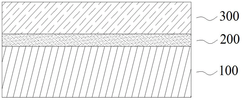
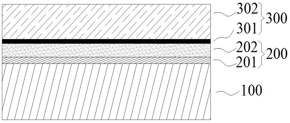
[0047] In this embodiment, a GaN thick film is grown on a SiC substrate to prepare a self-supporting GaN substrate. The structure of nitride epitaxial layer growth is as follows image 3 As shown, the initial substrate 100 is 6H-SiC, and the crystal plane direction is (0001); the oxide sacrificial layer 200 is a layer of LiAlO 2 single crystal film with a layer of LiGaO 2 The single crystal thin film is composed together: among them, 201 is LiAlO 2 Single crystal thin film; 202 is LiGaO 2 single crystal film. The nitride epitaxial layer 300 includes a thinner AlN buffer layer 301 and a thicker GaN thick film layer 302 .
[0048] The specific production method is as follows:
[0049] First, a clean 6H-SiC initial substrate is selected, and the substrate is polished on one side, and the crystal orientation of the polished surface is (0001). Then, the initial substrate was placed into a pulsed laser deposition (PLD) system to grow a layer of LiAlO with a thickness of 0.1 μm...
Embodiment 2
[0054] In this embodiment, a GaN substrate is selected as an initial substrate to fabricate an LED device wafer with a vertical structure. The epitaxial structure of the LED device wafer is as follows Figure 4 As shown, the order from bottom to top of the substrate is as follows: the initial substrate 100 is GaN, and the oxide sacrificial layer 200 is LiGaO 2 A single crystal thin film, a nitride epitaxial layer 300 is a nitride LED epitaxial layer, a p-type ohmic contact layer 400 , and a metal copper substrate 500 .
[0055] For the nitride LED epitaxial layer, its composition is: n-Al 0.3 Ga 0.7 N buffer layer 303 , n-GaN electron injection layer 304 , InGaN / GaN multi-quantum well active region 305 , p-GaN hole injection layer 306 . The specific manufacturing method of the vertical structure nitride LED device wafer is as follows:
[0056] In the first step, a clean GaN initial substrate is selected, and the substrate is polished on one side, and the crystal orientatio...
Embodiment 3
[0063] In this embodiment, a SiC substrate is selected as an initial substrate to manufacture a HEMT epitaxial device wafer, and the HEMT device wafer is transferred to a Si substrate for chip device processing. The epitaxial structure of the HEMT device wafer is as follows Figure 7 As shown, the initial substrate 100 is 4H-SiC with (0001) crystal plane orientation, and the sacrificial oxide layer 200 is NaGaO 2 Single crystal thin film, 307 is AlN nucleation layer, 308 is GaN buffer layer, 309 is extremely thin AlN intermediate layer, 310 is Al 0.3 Ga 0.7 N layers. The specific manufacturing method of the HEMT device wafer is as follows:
[0064] In the first step, the cleaned semi-insulating 4H-SiC initial substrate is selected, and the substrate is polished on one side, and the crystal orientation of the polished surface is (0001). Then, the initial substrate was put into a pulsed laser deposition (PLD) system, and a layer of NaGaO with a thickness of 0.2 μm was grown ...
PUM
| Property | Measurement | Unit |
|---|---|---|
| Thickness | aaaaa | aaaaa |
| Thickness | aaaaa | aaaaa |
| Thickness | aaaaa | aaaaa |
Abstract
Description
Claims
Application Information