
A kind of organic light-emitting display device and preparation method thereof

A light-emitting display and organic technology, applied in semiconductor/solid-state device manufacturing, semiconductor/solid-state device parts, semiconductor devices, etc., can solve the problems of metal oxide semiconductor thin film transistors, second electrode faults, etc., to reduce light Loss, increase the aperture ratio, and reduce the effect of process cost

Active Publication Date: 2017-08-04
CHENGDU VISTAR OPTEOLECTRONICS CO LTD
View PDF4 Cites 0 Cited by
  • Summary
  • Abstract
  • Description
  • Claims
  • Application Information

AI Technical Summary

Problems solved by technology

[0007] Therefore, what the present invention aims to solve is the technical problem that the metal oxide semiconductor thin film transistor cannot be used in the top-emitting organic light-emitting diode display device and easily causes the second electrode to be broken, and provides a new type of organic light-emitting display device and its preparation method

Method used


Image

  • A kind of organic light-emitting display device and preparation method thereof
  • A kind of organic light-emitting display device and preparation method thereof

Examples


Embodiment 1

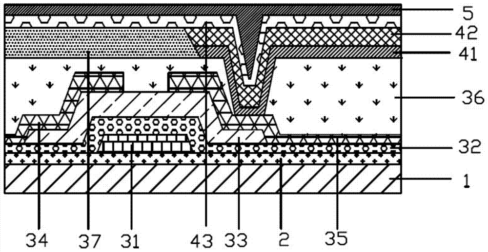
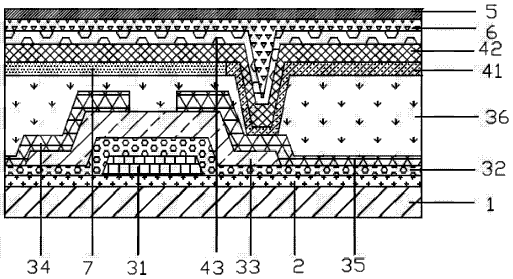
[0055] This embodiment provides an organic light emitting display device, such as figure 2 As shown, it includes a substrate 1 and a thin-film transistor arranged on the substrate 1. The thin-film transistor in this embodiment has a bottom-gate structure, and the thin-film transistor further includes a gate 31 and a gate insulating layer 32, a semiconductor layer 33, and a drain 34 and a source 35 arranged at both ends of the semiconductor layer 33; a passivation layer 36 is also arranged on the thin film transistor, and the passivation layer 36 includes a first electrode 41, an organic layer 42 and the organic light emitting diode of the second electrode 43, the passivation layer 36 is provided with a through hole connecting the source electrode 35 and the first electrode 41, and the second electrode 43 is sequentially provided with light extraction layer 6 and encapsulation layer 5; the semiconductor layer 33 is a metal oxide semiconductor layer, the passivation layer 36 is...


PUM


Abstract

The present invention provides an organic light-emitting display device. An ultraviolet blocking layer having a thickness equal to that of the first electrode is arranged on the passivation layer, which not only realizes the use of metal oxide semiconductor thin film transistors in top-emitting organic light-emitting diode devices, but also The ultraviolet blocking layer can play the role of the pixel definition layer; the metal oxide semiconductor is used as the semiconductor layer, and its carrier mobility is high, which can greatly improve the charge and discharge rate of the TFT to the pixel electrode, improve the response speed of the pixel, and achieve faster high refresh rate; the display device adopts a top-emission structure with a high aperture ratio; and it is provided with a light extraction layer. Under the synergy with the ultraviolet blocking layer, it can not only further block ultraviolet rays, but also reduce light loss caused by total reflection , further improving the luminous efficiency of the display device; the preparation process is simple and easy to implement.

Description

technical field [0001] The invention relates to the field of display, in particular to an organic light-emitting display device and a preparation method thereof. Background technique [0002] Active Matrix Organic Light Emitting Devices (English full name Active Matrix Organic Lighting Emitting Display, referred to as AMOLED), use thin film transistors (English full name Thin Film Transistor, referred to as TFT), with capacitor storage signals to control organic light emitting diodes (English full name Organic Lighting Emitting Diode , referred to as OLED) brightness and grayscale performance. Each individual AMOLED has a complete second electrode, an organic functional layer and a first electrode, and the first electrode covers an array of thin film transistors to form a matrix. The array of thin film transistors forms a circuit, which determines the lighting conditions of the pixels, and then determines the composition of the image. AMOLED can be large-sized, saves power...

Claims


Application Information

Patent Timeline
Patent Type & Authority Patents(China)
IPC IPC(8): H01L27/32H01L29/786H01L23/552H01L51/52H01L21/77
Inventor 敖伟邱勇黄秀颀
Owner CHENGDU VISTAR OPTEOLECTRONICS CO LTD
Learn More