TFET (Tunneling Field Effect Transistor) and forming method thereof

A tunneling field effect and transistor technology, which is applied in the fields of semiconductor devices, semiconductor/solid-state device manufacturing, electrical components, etc. The effect of increasing the current

Active Publication Date: 2015-03-18
SEMICON MFG INT (SHANGHAI) CORP
View PDF6 Cites 6 Cited by
  • Summary
  • Abstract
  • Description
  • Claims
  • Application Information

AI Technical Summary

Problems solved by technology

[0006] The problem solved by the invention is that in the prior art, the operating ...

Method used


Image

  • TFET (Tunneling Field Effect Transistor) and forming method thereof
  • TFET (Tunneling Field Effect Transistor) and forming method thereof
  • TFET (Tunneling Field Effect Transistor) and forming method thereof

Examples


no. 1 example

[0077] This embodiment provides a method for forming a tunneling field effect transistor, including:

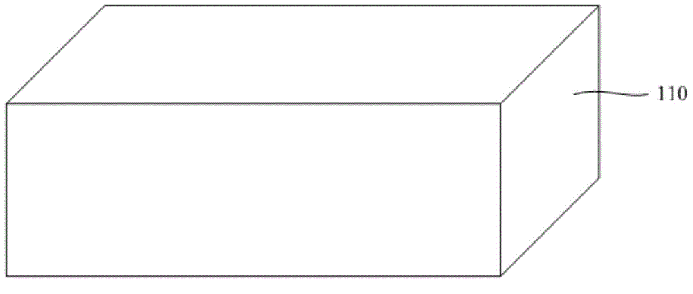
[0078] refer to figure 2 , providing a substrate 110 .

[0079] The substrate 110 may be a silicon substrate, a silicon germanium substrate or other semiconductor substrates known in the art.

[0080] In this embodiment, the substrate 110 is not doped.

[0081] In other embodiments, the second type of doping can be performed on the bottom of the substrate 110 first, and a deep doped well is formed at the bottom of the substrate 110; then, the first type of doping is performed on the substrate 110 above the deep doped well. impurity, forming the first type doped well. The first type of doping and the second type of doping are different.

[0082] The purpose of forming deep doped wells and first type doped wells is to avoid latch-up and other reliability problems.

[0083] In this embodiment, the first type of doping is p-type, and the second type of doping is n-type.

...

no. 2 example

[0152] The difference between this embodiment and the first embodiment is:

[0153] refer to Figure 9 , after forming the source 161, on the upper surface of the substrate 110, the gate structure, the channel fin 130 and the source 161, and the gate structure, the underlying fin 120, the channel fin 130 and the source 161 The sidewalls form a mask layer having a window exposing the channel fin 130 and the underlying fin 120 on the other side of the gate structure;

[0154] performing heavily doped ion implantation on the channel fin 130 through the window to form a drain 162 in the channel fin 130;

[0155] removing the second patterned mask layer.

[0156] In other embodiments, the drain 162 may also be formed first, and then the source 161 is formed.

[0157] The method for forming the TFET is described above by taking the source 161 across the channel fin 130 on one side of the gate structure as an example.

[0158] In other embodiments, heavily doped ion implantation ...

no. 3 example

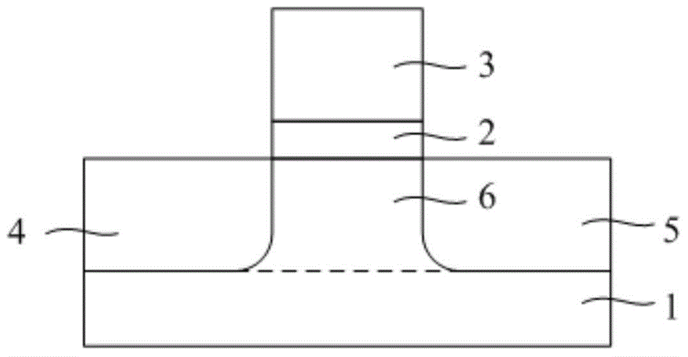
[0162] refer to Figure 8 , this embodiment provides a tunneling field effect transistor, including:

[0163] base 110;

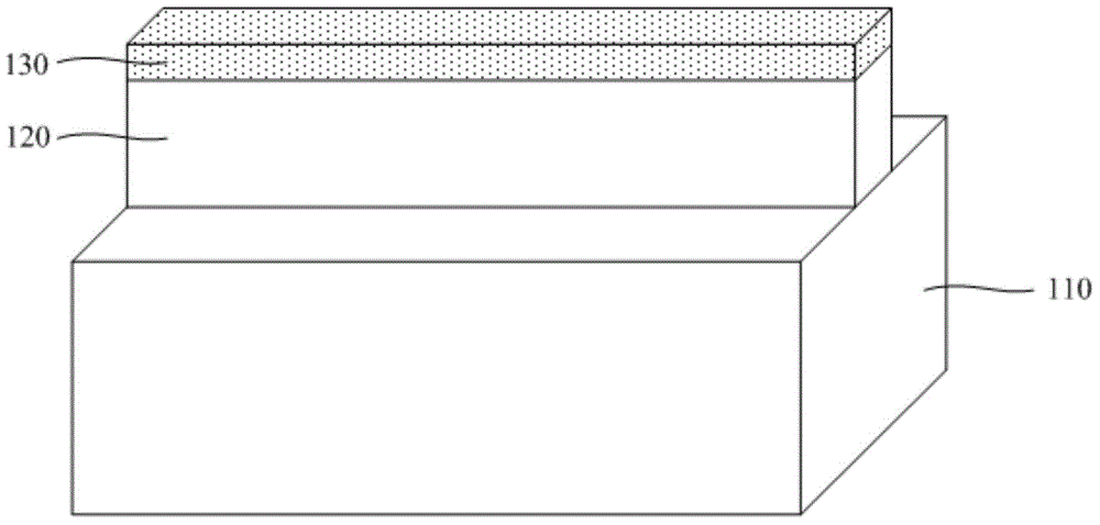
[0164] a bottom fin 120 on the substrate 110, the bottom fin 120 has a first type of doping;

[0165] The channel fin 130 located on the upper surface of the bottom fin 120, the channel fin 130 has a second type of doping, the second type of doping is different from the first type of doping, the channel fin 130 The electron mobility of is greater than the electron mobility of the bottom fin 120;

[0166] a gate structure spanning the channel fin;

[0167] a source 161 having a first type of doping;

[0168] The drain 162 has the second type of doping.

[0169] The source 161 straddles the channel fin 130 . In other embodiments, the source 161 may also be located in the channel fin 130 .

[0170] The drain 162 straddles the channel fin 130 . In other examples, refer to Figure 9 , the drain 162 may also be located in the channel fin 130 .

[0171] ...


PUM

PropertyMeasurementUnit
Thicknessaaaaaaaaaa

Abstract

The invention discloses a TFET (Tunneling Field Effect Transistor) and forming method thereof. The TFET comprises a substrate, a bottom-layer fin part, a channel fin part, a gate structure, a source electrode and a drain electrode, wherein the bottom-layer fin part is positioned on the substrate and is provided with a first type of doping; the channel fin part is positioned on the upper surface of the bottom-layer fin part and is provided with a second type of doping, the second type of doping is different from the first type of doping, and the electron mobility of the channel fin part is greater than that of the bottom-layer fin part; the gate structure stretches across the channel fin part; the source electrode is provided with the first type of doping; the drain electrode is provide with the second type of doping. The TFET provided by the invention has high working current and low power consumption.

Description

technical field [0001] The invention relates to the field of semiconductors, in particular to a tunneling field effect transistor and a forming method thereof. Background technique [0002] Metal-Oxide-Semiconductor (MOS) technology has been widely used. For example, Complementary Metal Oxide Semiconductor (CMOS) transistors have become core components in semiconductor integrated circuits. In order to continuously improve the performance and packaging density of integrated circuits, and to reduce the cost of integrated circuits, the feature size of CMOS transistors is continuously reduced. [0003] However, as the dimensions of CMOS transistors continue to shrink, the overall power consumption of CMOS transistors continues to increase. The reasons are as follows: 1. The short channel effect becomes more and more obvious (such as the leakage current increases); 2. It is difficult to make the power supply voltage continue to decrease as the size of the CMOS transistor decreas...

Claims


Application Information

Patent Timeline
IPC IPC(8): H01L29/78H01L29/08H01L21/336
CPCH01L29/0843H01L29/66477H01L29/78
Inventor 黄新运曾以志孙浩
Owner SEMICON MFG INT (SHANGHAI) CORP
Why Eureka
Try Eureka