Organic electroluminescent device and preparation method thereof
An electroluminescent device and electroluminescent technology, which are applied in the fields of electro-solid devices, semiconductor/solid-state device manufacturing, electrical components, etc., and can solve the problems of refractive index difference, total reflection loss, low light extraction efficiency, etc.
- Summary
- Abstract
- Description
- Claims
- Application Information
AI Technical Summary
Problems solved by technology
Method used
Image
Examples
preparation example Construction
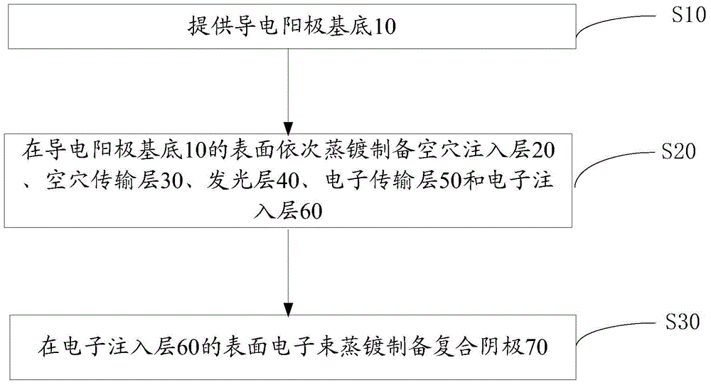
[0040] Please also see figure 2 , the preparation method of above-mentioned organic electroluminescent device, it comprises the following steps:
[0041] Step S10 , providing a conductive anode substrate 10 .
[0042] The conductive anode substrate 10 is indium tin oxide glass (ITO), aluminum zinc oxide glass (AZO) or indium zinc oxide glass (IZO), preferably ITO.
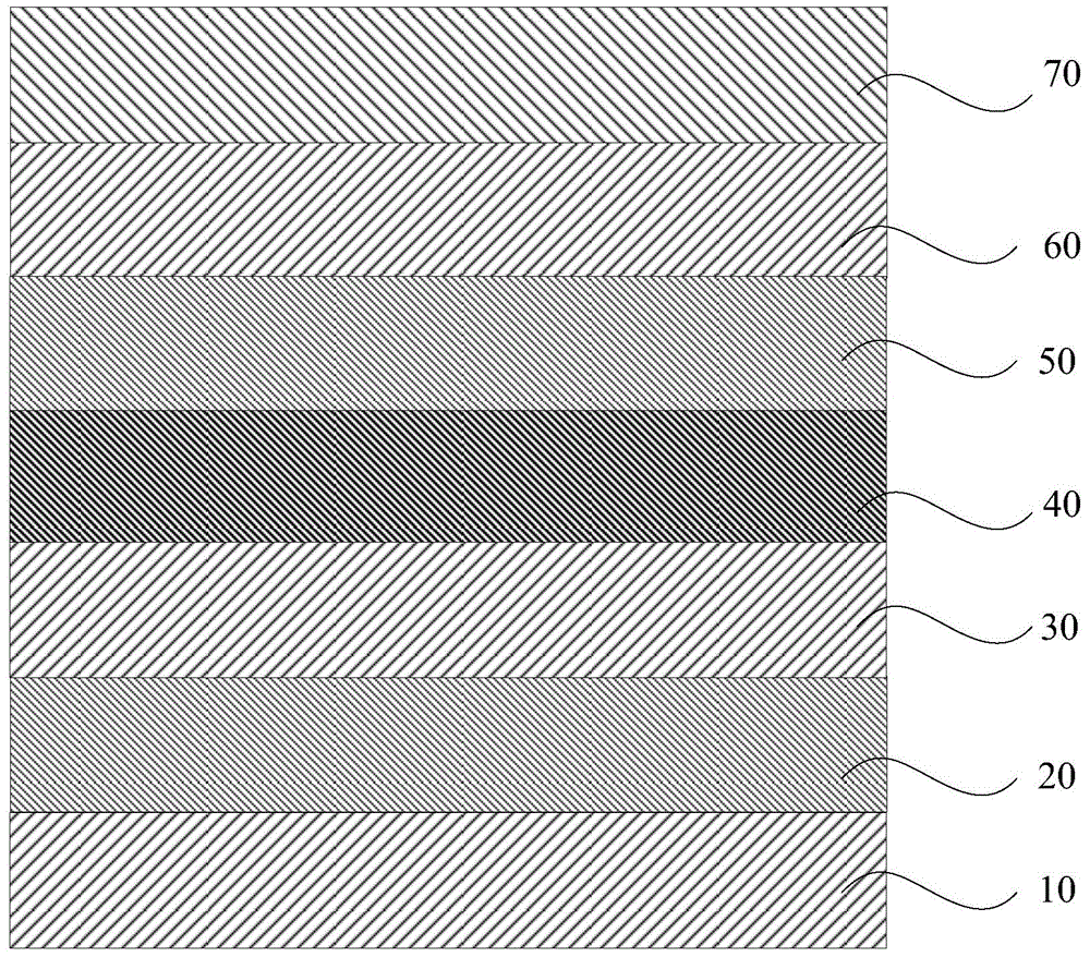
[0043] Step S20 , the hole injection layer 20 , the hole transport layer 30 , the light emitting layer 40 , the electron transport layer 50 and the electron injection layer 60 are sequentially evaporated on the surface of the conductive anode substrate 10 .
[0044] Before the hole injection layer 20 is prepared by vapor deposition on the surface of the conductive anode substrate 10, the following operations are also included: after the conductive anode substrate 10 is photolithographically trimmed, sequentially wash with detergent, deionized water, acetone, ethanol and isopropanol Ultrasonic treatment for 15min. ...
Embodiment 1
[0063] The structure prepared in this example is ITO glass / MoO 3 / TCTA / Alq 3 / TAZ / LiF / Ca:FeCl 3 :Al 2 o 3 organic electroluminescent devices. Among them, " / " means cascading, and ":" means mixing.
[0064] Provide ITO glass as a conductive anode substrate, cut the ITO glass by photolithography, and then use detergent, deionized water, acetone, ethanol and isopropanol to ultrasonically treat for 15 minutes to remove contamination.
[0065] The working pressure is 8×10 -5 Pa, the evaporation rate of organic materials is 0.2nm / s, and the evaporation rate of metals and metal compounds is 3nm / s, the hole injection layer, the hole transport layer, and the luminescent layer are sequentially evaporated on the surface of ITO glass. layer, electron transport layer and electron injection layer. The material of the hole injection layer is MoO 3 , with a thickness of 40nm. The material of the hole transport layer is TCTA, and the thickness is 50nm. The material of the light-emitt...
Embodiment 2
[0071] The structure prepared in this example is AZO glass / V 2 o 5 / TCTA / ADN / TAZ / CsF / Mg:FeBr 3 :SiO2 2 organic electroluminescent devices. Among them, " / " means cascading, and ":" means mixing.
[0072] AZO glass was provided as the conductive anode substrate, and after the AZO glass was photolithographically cut, it was sequentially treated with detergent, deionized water, acetone, ethanol, and isopropanol for 15 minutes to remove contamination.
[0073] The working pressure is 2×10 -3 Pa, the evaporation rate of organic materials is 0.1nm / s, and the evaporation rate of metals and metal compounds is 10nm / s, the hole injection layer, the hole transport layer, and the luminescent layer are sequentially evaporated on the surface of AZO glass. layer, electron transport layer and electron injection layer. The material of the hole injection layer is V2O5, and the thickness is 80nm. The material of the hole transport layer is TCTA, and the thickness is 60nm. The material of ...
PUM
| Property | Measurement | Unit |
|---|---|---|
| thickness | aaaaa | aaaaa |
| thickness | aaaaa | aaaaa |
| thickness | aaaaa | aaaaa |
Abstract
Description
Claims
Application Information


