High-precision and interval-controllable electrode and preparing method thereof
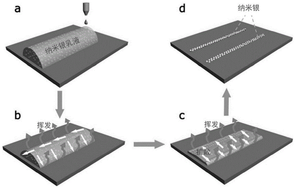
A high-precision, spacing technology, used in cable/conductor manufacturing, circuits, electrical components, etc., can solve problems such as high cost, large amounts of heavy metals and waste water, and living environment pollution, and achieve accelerated research and development progress, rapid preparation, and low cost. Effect
- Summary
- Abstract
- Description
- Claims
- Application Information
AI Technical Summary
Problems solved by technology
Method used
Image
Examples
Embodiment 1
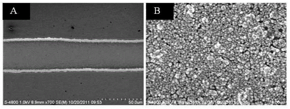
[0032] A high-precision electrode circuit with a line width of about 5 μm and a spacing of about 70 μm is prepared on the surface of a high-temperature-resistant polyester (PET) substrate, and is used to study the preparation of large-size transparent conductive films by the grid method (MetalMesh).
[0033] (1) At first, a pattern arranged alternately by high surface energy regions and low surface energy regions is prepared on the surface of PET. The low surface energy regions are fluorosilanes with a thickness of 500 nm, and the high surface energy regions are the intrinsic surfaces of PET. It is 80 μm; the contact angle of the low surface energy region is 69.4°; the contact angle of the high surface energy region is 125.5°;
[0034] (2) Disperse 2g of conductive polymer poly-3,4-ethylenedioxythiophene and polystyrene sulfonate mixture (Bayer AG company) in 98g of water to prepare a conductive polymer solution with a solid content of 2wt%;
[0035] (3) Cover the high surface...
Embodiment 2
[0038] Transistor electrodes with a line width of about 10 μm and a spacing of about 80 μm, 120 μm, 160 μm and 200 μm were prepared on the surface of single crystal silicon to study the effect of electrode spacing on the performance of organic transistors.
[0039] (1) First prepare a pattern of high surface energy regions and low surface energy regions alternately arranged on the surface of single crystal silicon, the low surface energy region is C12 perfluoroalkane with a thickness of 300nm deposited at 190°C, and the high surface energy region It is the intrinsic surface of monocrystalline silicon, and its width is 100 μm, 140 μm, 180 μm and 220 μm; the contact angle of the low surface energy region is 39.7°; the contact angle of the high surface energy region is 127.7°;
[0040] (2) 4g particle size scope is that the nano-silver of 30-50nm is dispersed in 96g water, makes solid content and is 4wt% nano-silver emulsion;
[0041] (3) Spread the nano-silver emulsion all over ...
Embodiment 3
[0044] Blood glucose electrochemical sensor electrodes with a line width of about 20 μm and a spacing of about 500 μm were prepared on the surface of polyvinyl chloride (PVC) film.
[0045] (1) First prepare a pattern on the surface of the PVC film alternately arranged by high surface energy regions and low surface energy regions, and the low surface energy region is a mixed coating of fluorosilane and nano-silicon dioxide (particle size 20nm) with a thickness of 800nm , the high surface energy region is the intrinsic surface of the PVC film, and its width is 540 μm; the contact angle of the low surface energy region is 48.3°; the contact angle of the high surface energy region is 148.4°;
[0046] (2) Dispersing 8g of nano-gold with a particle size range of 5-10nm in 92g of water to prepare a solid content of 8wt% nano-gold emulsion;
[0047] (3) Spread the nano-gold emulsion all over the high surface energy area, and continue heating at 45°C for 10 minutes, so that the nano-g...
PUM
| Property | Measurement | Unit |
|---|---|---|
| thickness | aaaaa | aaaaa |
| thickness | aaaaa | aaaaa |
| width | aaaaa | aaaaa |
Abstract
Description
Claims
Application Information


