Method for making gallium nitride high electron-mobility transistor on silicon slice

A technology with high electron mobility and electron mobility, applied in circuits, electrical components, semiconductor devices, etc., to achieve high quality, simple process, and good compatibility

Inactive Publication Date: 2015-03-25
NO 55 INST CHINA ELECTRONIC SCI & TECHNOLOGYGROUP CO LTD
View PDF6 Cites 6 Cited by
  • Summary
  • Abstract
  • Description
  • Claims
  • Application Information

AI Technical Summary

Problems solved by technology

[0006] The purpose of the present invention is to solve the problem that current heteroepitaxy and other methods cannot realize the fabrication of gallium nitride high electron mobility transistors on the Si (100) surface, and propose a method of using epitaxial transfer to realize silicon substrates based on Si (100) crystal planes. The new method for the preparation of gallium nitride high electron mobility transistors can break through the inherent limitation of the lattice constant mismatch of different materials, ensuring the quality of the gallium nitride epitaxial layer and the high performance of the device

Method used


Image

  • Method for making gallium nitride high electron-mobility transistor on silicon slice
  • Method for making gallium nitride high electron-mobility transistor on silicon slice
  • Method for making gallium nitride high electron-mobility transistor on silicon slice

Examples


Embodiment

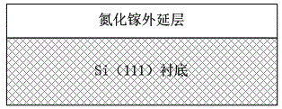
[0039] ① Thoroughly clean the Si (111) substrate, and then use metal organic chemical vapor deposition (MOCVD) to grow the epitaxial layer material of gallium nitride high electron mobility transistor on the Si (111) surface;

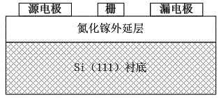
[0040] ② Conduct semiconductor process fabrication of GaN HEMT devices on the above-mentioned gallium nitride-on-silicon wafer;

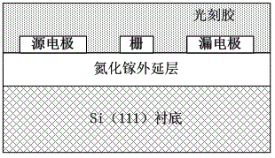
[0041] ③The photoresist is spin-coated on the front side, the speed is 2000 rpm, the acceleration is 2000 rpm, and the spin-coating time is 90 seconds; the GaN HEMT wafer coated with the photoresist faces up on the heating plate, and the temperature of the hot plate is 110 degrees Celsius, baking time 2 minutes;

[0042] ④ Take the GaN HEMT wafer out of the hot plate and stack it with the front of the glass sheet, fix it with a fixture and put it into a bonding machine for bonding. The bonding force is 4000N, and the bonding time is 60 minutes. GaN HEMTs bonded to temporary mounts;

[0043] ⑤ Take 100ml of analytically pure...


PUM


Abstract

The invention provides a method for making a gallium nitride high electron-mobility transistor on a silicon slice of a crystal face (100). The method includes the steps that (1) an epitaxial layer material of the gallium nitride high electron-mobility transistor grows on the silicon slice of a crystal face (111) through MOCVD in an epitaxial mode; (2) the making process of the gallium nitride high electron-mobility transistor is conducted; (3) spin coating and etching are conducted on a rubber protection device structure, and a wafer is temporarily arranged on a carrier piece in a bonding mode; (4) corrosion is conducted, (5) the exposed gallium nitride epitaxial layer is provided with a BCB in a spin coating mode; (6) natural cooling is conducted and thermocompression bonding is conducted in a bonder; (7) the temporary carrier piece is removed, and the front face of the wafer is cleaned thoroughly. The method has the advantages that the gallium nitride high electron-mobility transistor can be made on the face of the Si (100), the process is simple, the yield is high, and the problem that due to lattice mismatch, the epitaxial layer material of the gallium nitride high electron-mobility transistor cannot grow on the face of the Si (100) directly in an epitaxial mode is solved.

Description

technical field [0001] The invention relates to a method for manufacturing a gallium nitride high electron mobility transistor on a silicon wafer of Si (100) crystal plane, belonging to the technical field of semiconductor technology. Background technique [0002] As a third-generation semiconductor material, gallium nitride has excellent characteristics such as wide band gap and high electron saturation velocity. Therefore, high electron mobility transistors made of gallium nitride materials have the characteristics of high speed and high power. Gallium nitride materials are mainly obtained by heterogeneous epitaxial growth methods, and expensive silicon carbide is used as the epitaxial substrate, which has a high cost and limits the development of gallium nitride materials. Gallium nitride epitaxial materials based on silicon (Si) substrates have the advantages of low cost and large size, so they have attracted the attention of scholars at home and abroad. [0003] In add...

Claims


Application Information

Patent Timeline
Patent Type & Authority Applications(China)
IPC IPC(8): H01L21/335
CPCH01L29/66431
Inventor 赵岩吴立枢程伟孔岑
Owner NO 55 INST CHINA ELECTRONIC SCI & TECHNOLOGYGROUP CO LTD
Why Eureka
Try Eureka