Thin film transistor low-temperature polycrystalline silicon thin film manufacturing method

A thin-film transistor and low-temperature polysilicon technology, which is applied in the manufacture of transistors, semiconductor/solid-state devices, semiconductor devices, etc., can solve the problems of increasing the production cost of flat-panel displays, different numbers of grain boundaries, and uneven device performance.

Inactive Publication Date: 2015-03-25
TRULY HUIZHOU SMART DISPLAY
View PDF3 Cites 11 Cited by
  • Summary
  • Abstract
  • Description
  • Claims
  • Application Information

AI Technical Summary

Problems solved by technology

The inventor found in the research that the number of grain boundaries contained in the TFT channel is different when the low-temperature polysilicon film is used in the traditional technology, which will cause the problem of uneven device performance, and its carrier mobility can be further improved
To solve this problem, of course, monocrystalline silicon thin films can be used to replace polycrystalline silicon thin films, but this will increase the cost of flat panel display manufacturing

Method used


Image

  • Thin film transistor low-temperature polycrystalline silicon thin film manufacturing method
  • Thin film transistor low-temperature polycrystalline silicon thin film manufacturing method
  • Thin film transistor low-temperature polycrystalline silicon thin film manufacturing method

Examples


Embodiment Construction

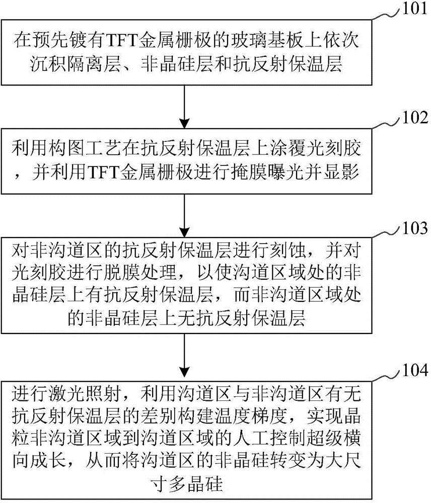
[0041] In order to make the object, technical solution and advantages of the present invention clearer, the present invention will be further described in detail below in conjunction with the accompanying drawings and embodiments. It should be understood that the specific embodiments described here are only used to explain the present invention, not to limit the present invention.

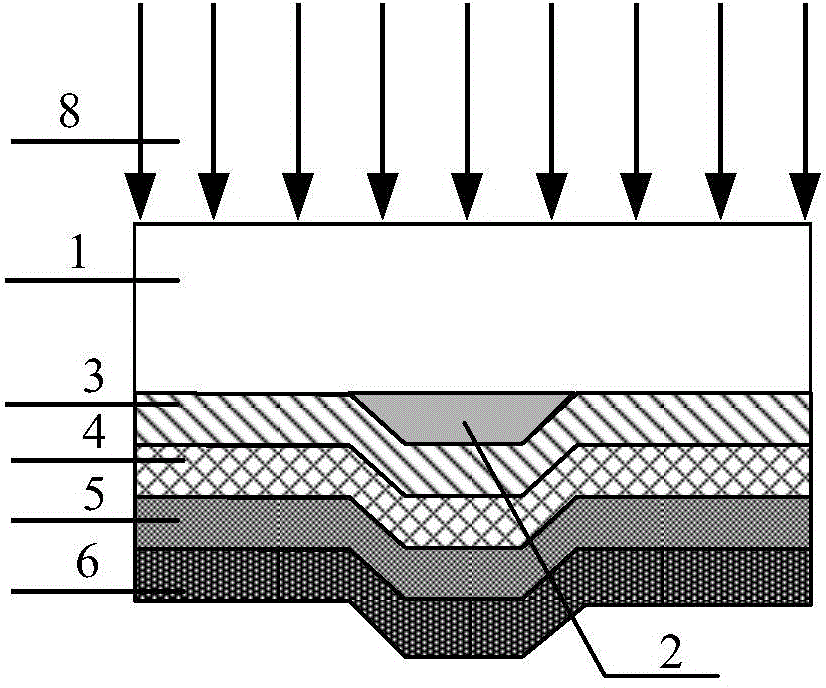
[0042] see figure 1 , Figure 2(A) to Figure 2(C) , In one embodiment, a method for preparing a low-temperature polysilicon thin film for a thin film transistor is provided. The method is applied in the preparation process of a thin film transistor with an inverted gate structure, and the method includes:

[0043] Step 101 , depositing an isolation layer, an amorphous silicon layer and an anti-reflection insulation layer in sequence on the glass substrate pre-plated with a TFT metal gate.

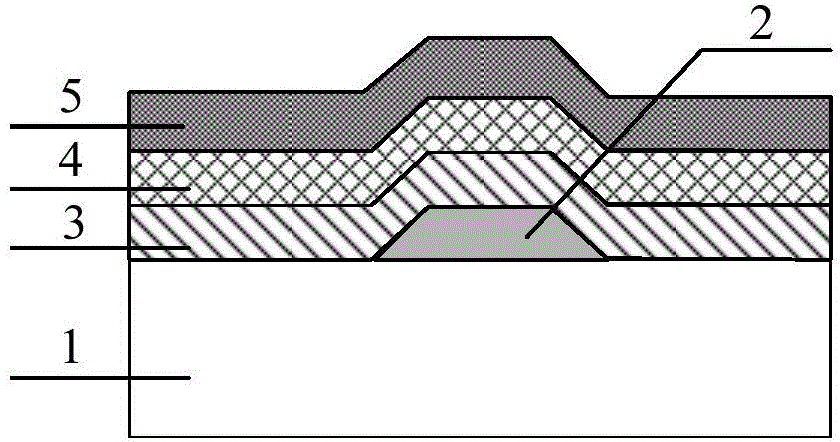
[0044] Specifically, as shown in FIG. 2(A), during the preparation process of the thin film transistor wit...


PUM


Abstract

The invention discloses a thin film transistor low-temperature polycrystalline silicon thin film manufacturing method. The method includes the steps of firstly, sequentially depositing an isolation layer, a non-crystalline silicon layer and an anti-reflection heat preservation layer on a glass substrate where a TFT metal grid is plated in advance; secondly, coating the anti-reflection heat preservation layer with photoresist through a picture composition process, and conducting mask exposure and developing through the TFT metal grid; thirdly, etching the portion, in a non-channel area, of the anti-reflection heat preservation layer, and conducting demolding on the photoresist; fourthly, conducting laser radiation so that the non-crystalline silicon of a channel area can be converted into large-size polycrystalline silicon. By means of the technical scheme, the temperature gradient of the TFT channel area and the non-channel area can be formed, the manual-control super transverse growth of crystalline grain from the non-channel area to the channel area can be achieved, the TFT channel area has only one grain boundary, and therefore the carrier migration rate is increased, and the performance of a device in a channel is uniform.

Description

technical field [0001] The invention relates to the technical field of semiconductor device preparation, in particular to a method for preparing a low-temperature polysilicon film for a thin film transistor. Background technique [0002] Polycrystalline silicon (p-Si) thin film has a high carrier mobility much larger than that of amorphous silicon (a-Si) and comparable to that of single crystal silicon, and is often used in active TFT (Thin Film Transistor) Layers, for example, have very important applications in active liquid crystal displays (AMOLCDs) and active organic light emitting diodes (AMOLEDs). [0003] The substrate of the polysilicon thin film of the flat panel display is usually glass which cannot withstand the high temperature process. Under the limitation of this condition, the industry must choose to develop the low temperature polysilicon (LTPS) technology. In research, the inventors found that the low-temperature polysilicon film used in the traditional te...

Claims


Application Information

Patent Timeline
Patent Type & Authority Applications(China)
IPC IPC(8): H01L21/336
CPCH01L29/6675H01L29/786H01L29/78672
Inventor 陈卓陈建荣任思雨苏君海黄亚清李建华
Owner TRULY HUIZHOU SMART DISPLAY
Why Eureka
Try Eureka