Photoelectric conversion method used for nano junction type photovoltaic device

A photoelectric conversion and photovoltaic device technology, applied in photovoltaic power generation, semiconductor devices, circuits, etc., can solve the problems of low power generation efficiency and consumption, and achieve the effects of simple structure, enhanced photovoltaic effect, and convenient production

Inactive Publication Date: 2015-03-25
SHANGHAI DIANJI UNIV
View PDF3 Cites 4 Cited by
  • Summary
  • Abstract
  • Description
  • Claims
  • Application Information

AI Technical Summary

Problems solved by technology

However, the current power generation efficiency of semiconductor solar cells is still low, and a large amount of light energy absorbed in the power generation process is consumed in the form of heat, which is one of the key bottlenecks restricting the substantial improvement of photoelectric conversion efficiency and obtaining large photoelectric power

Method used


Image

  • Photoelectric conversion method used for nano junction type photovoltaic device
  • Photoelectric conversion method used for nano junction type photovoltaic device

Examples


Embodiment Construction

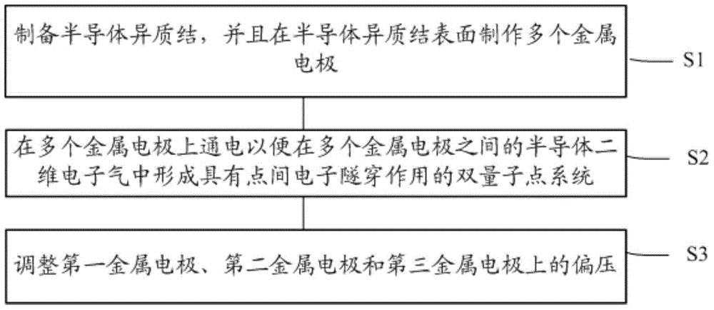
[0023] In order to make the content of the present invention clearer and easier to understand, the content of the present invention will be described in detail below in conjunction with specific embodiments and accompanying drawings.

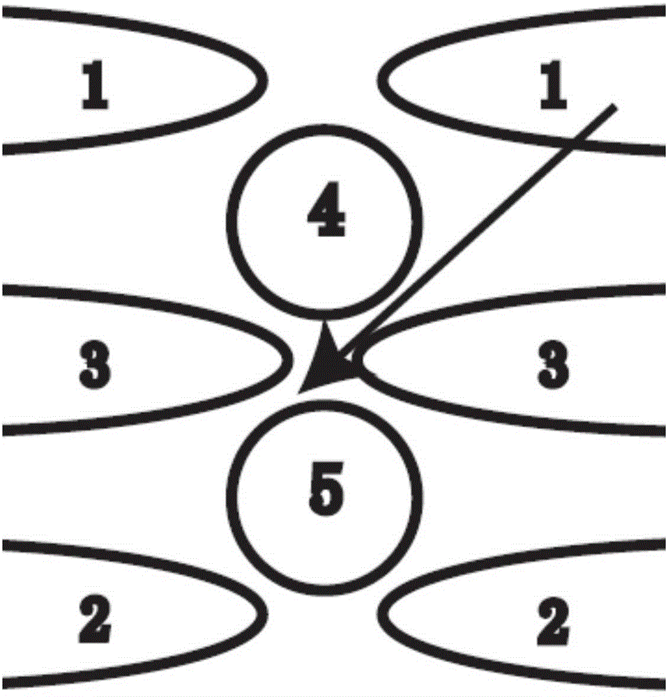
[0024] figure 1 Schematically showing a flow chart of a photoelectric conversion method for a nanojunction photovoltaic device according to a preferred embodiment of the present invention; figure 2 A schematic diagram of a photoelectric conversion method for a nanojunction photovoltaic device according to a preferred embodiment of the present invention is schematically shown.

[0025] Such as figure 1 and figure 2 As shown, the photoelectric conversion method for nano-junction photovoltaic devices according to a preferred embodiment of the present invention includes:

[0026] The first step S1 is used to prepare a semiconductor heterojunction, and fabricate a plurality of metal electrodes for controlling quantum dots on the surface of the s...


PUM


Abstract

A photoelectric conversion method used for a nano junction type photovoltaic device includes the steps that a semiconductor heterojunction is prepared, a first metal electrode, a second metal electrode and a third metal electrode are manufactured on the surface of the semiconductor heterojunction and sequentially arranged in parallel, and each metal electrode comprises two electrode parts which are spaced and arranged oppositely; the metal electrodes are powered on so as to form a double-quantum-dot system; a first semiconductor quantum dot is formed between the first metal electrode and the second metal electrode, and a second semiconductor quantum dot is formed between the second metal electrode and the third metal electrode; the bias voltage on the first metal electrode, the second metal electrode and the third metal electrode is adjusted, so that only two single electron states of the double-quantum-dot system work when the double-quantum-dot system conducts electricity, wherein the double-quantum-dot system comprises the first semiconductor quantum dot and the second semiconductor quantum dot, only one excitation electron exists in the double-quantum-dot system at most when the double-quantum-dot system conducts the electricity, and the excitation electron absorbs photons with preset energy under the action of tunneling between dots.

Description

technical field [0001] The present invention relates to the application field of renewable clean energy, in particular to the field of semiconductor photovoltaic devices; more specifically, the present invention relates to a photoelectric conversion method for nano junction photovoltaic devices. Background technique [0002] In recent years, coal-based thermal power generation, which accounts for more than 80% of my country's annual power generation, is one of the culprits in causing environmental problems such as smog, seriously affecting people's daily life and even their physical and mental health. Not only that, the modern society with oil, natural gas, and coal as the main energy sources is facing the threat of fossil energy depletion. Therefore, it has become a social consensus to vigorously develop new energy sources such as nuclear power, hydropower, wind power, and solar energy. [0003] As a renewable and clean energy source, solar energy is becoming more and more...

Claims


Application Information

Patent Timeline
Patent Type & Authority Applications(China)
IPC IPC(8): H01L31/0352H01L31/0735H01L31/18
CPCH01L31/035218H01L31/0735H01L31/18Y02E10/544Y02P70/50
Inventor 钟旭
Owner SHANGHAI DIANJI UNIV
Why Eureka
Try Eureka