Wafer-level fan-out PoP encapsulation structure and making method thereof

A packaging structure, wafer-level technology, applied in semiconductor/solid-state device manufacturing, electrical components, electrical solid-state devices, etc.

Inactive Publication Date: 2015-04-08
HUATIAN TECH XIAN
View PDF8 Cites 16 Cited by
  • Summary
  • Abstract
  • Description
  • Claims
  • Application Information

AI Technical Summary

Problems solved by technology

[0004] The present invention proposes a packaging structure and manufacturing method for the three-dimensional PoP packaging

Method used


Image

  • Wafer-level fan-out PoP encapsulation structure and making method thereof
  • Wafer-level fan-out PoP encapsulation structure and making method thereof
  • Wafer-level fan-out PoP encapsulation structure and making method thereof

Examples


Embodiment Construction

[0045]In order to make the purpose, technical solution and advantages of the present invention clearer, the specific implementation manners of the present invention will be further described in detail below in conjunction with the accompanying drawings.

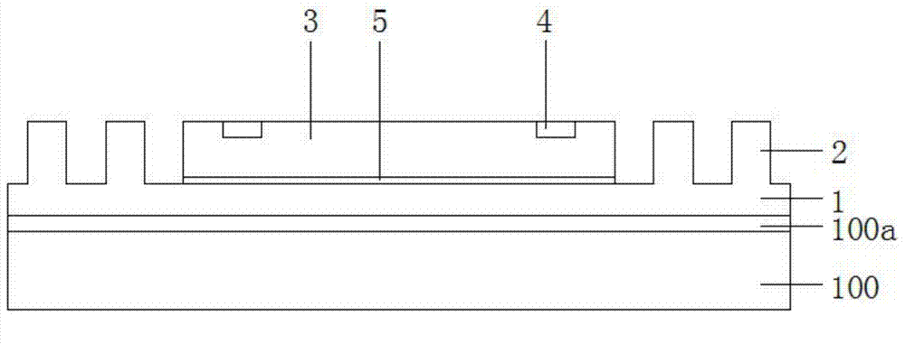
[0046] Such as Figure 14 As shown, a wafer-level fan-out PoP packaging structure is formed by stacking at least one fan-out PoP packaging unit; a fan-out PoP packaging unit is composed of two packages with the same structure;

[0047] The one package includes a metal bump structure 2, an IC chip 3, a bonding pad 4, a second paste material 5, a first plastic packaging material 6, a first rewiring metal wiring layer 7, and a first metal layer 8 , the first dielectric material layer 9, the second rewiring metal wiring layer 10, the second dielectric material layer 11, the second metal layer 12; the IC chip 3 has a bonding pad 4, and the second paste material 5 is pasted on the surface of the IC chip 3, the first plastic encaps...


PUM


Abstract

The invention discloses a wafer-level fan-out PoP encapsulation structure and a making method thereof. The wafer-level fan-out PoP encapsulation structure is formed by stacking at least one fan-out PoP encapsulation units, each two adjacent fan-out PoP encapsulation units are connected through a second welding ball and coated and sealed by adopting a second plastic sealing material, each fan-out PoP encapsulation unit comprises an IC chip, a first plastic sealing material, a second binding material, a metal salient point structure, a first metal layer, a second metal layer, a first rewiring metal routing layer, a first dielectric material layer, a second rewiring metal routing layer, a second dielectric material layer, a first welding ball and the second welding ball, a bonding pad of each IC chip is connected with the corresponding first rewiring metal routing layer, each metal salient point structure forms a molded plastic through hole, and three-dimensional integrated interconnection between an upper encapsulating body as well as a lower encapsulating body in each fan-out PoP encapsulation unit and an external structure is realized through the corresponding molded plastic through hole. The making method mainly includes arranging a metal substrate wafer on a first carrier wafer; making the metal salient point structure on the surface of the metal substrate wafer; feeding the chip; plastically sealing, making the first rewiring metal routing layer; arranging a second carrier wafer, removing the first carrier wafer, etching the lower surface of the metal substrate wafer to form the second rewiring metal routing layer; performing stacking and reflow soldering; removing the second carrier wafer; forming the fan-out PoP encapsulation unit after ball placing and reflow soldering processes; performing stacking and reflow soldering on the fan-out PoP encapsulation units; and forming the wafer-level fan-out PoP encapsulation structure after plastic sealing. By the wafer-level fan-out PoP encapsulation structure and the making method, the problems of encapsulating density, cost and reliability of existing PoP encapsulation technology are solved.

Description

technical field [0001] The invention relates to the field of microelectronic packaging technology and three-dimensional integration technology, in particular to a three-dimensional wafer-level fan-out PoP packaging technology and a manufacturing method thereof. Background technique [0002] With the continuous development of electronic packaging products in the direction of high density, multi-function, low power consumption, and miniaturization, the system-in-package (SiP) using three-dimensional integration technology has achieved rapid development. The Through Silicon Via (TSV) technology solution is the optimal solution for realizing 3D integration technology due to its characteristics of the highest stacking density, the smallest size, greatly improved chip speed and reduced power consumption. However, the current TSV technology faces serious problems such as manufacturing difficulty, process cost, yield rate and reliability of finished products. The existing mature th...

Claims


Application Information

Patent Timeline
IPC IPC(8): H01L23/495H01L21/60
CPCH01L25/105H01L25/50H01L2224/0401H01L2224/04105H01L2224/12105H01L2224/16225H01L2224/19H01L2224/25H01L2224/2518H01L2224/32225H01L2224/73204H01L2224/73267H01L2224/81005H01L2224/81815H01L2224/92125H01L2225/1035H01L2225/1058H01L2924/181H01L2924/00H01L2924/00012
Inventor 夏国峰于大全
Owner HUATIAN TECH XIAN
Why Eureka
Try Eureka