
Method for preparing wafer-grade large-size hexagonal boron nitride on substrate

A hexagonal boron nitride, wafer-level technology, applied in gaseous chemical plating, metal material coating process, coating, etc., can solve the problems of small area of ​​hexagonal boron nitride, low coverage, poor uniformity, etc. , to achieve the effect of large output

Active Publication Date: 2015-04-22
XIAMEN UNIV
View PDF3 Cites 19 Cited by
  • Summary
  • Abstract
  • Description
  • Claims
  • Application Information

AI Technical Summary

Problems solved by technology

[0005] The purpose of the present invention is to solve the problems of small area, low coverage and poor uniformity of the existing hexagonal boron nitride, and to provide a large-area, high-quality, precise and controllable layer thickness method for preparing wafer-level large Dimensional Hexagonal Boron Nitride Method

Method used


Image

  • Method for preparing wafer-grade large-size hexagonal boron nitride on substrate
  • Method for preparing wafer-grade large-size hexagonal boron nitride on substrate
  • Method for preparing wafer-grade large-size hexagonal boron nitride on substrate

Examples


Embodiment 1

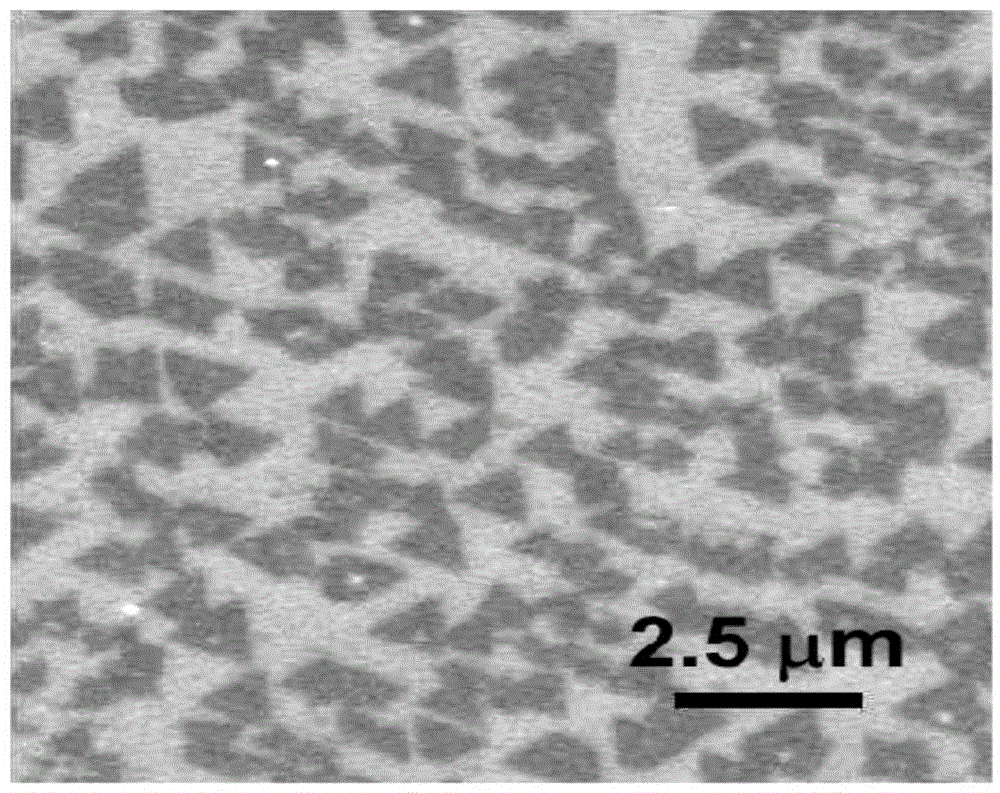
[0023] First, hexagonal boron nitride is grown controllably on Cu foil.

[0024] 1) Put 0.5mg Borazane powder in a quartz boat into a slender quartz tube, and put it into a three-temperature zone CVD device, such as figure 1 shown. Adjust the position so that the Borazane powder is in the middle of the first temperature zone, connect the slender small quartz tube to the vent, and then put the cleaned Cu foil into the third temperature zone of the CVD device, and ensure that it is in the third temperature zone. In the middle of the temperature zone, there are Borazane powder and Cu foil in sequence along the direction of airflow. The vacuum chamber is sealed with a rubber ring flange, and the predetermined temperature rise parameters and ventilation parameters are input into the computer to prepare for the subsequent heating of the three temperature zones of CVD. Start to vacuumize the cavity, first use a mechanical oil pump until the vacuum reaches 2×10 -2 At Torr, turn on ...

Embodiment 2

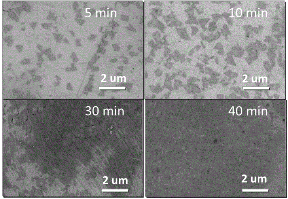
[0027] Example 2: Growing large-area continuous boron nitride

[0028] 1) As in Example 1, put the precursor into a 1mg Borazane powder in a quartz boat and place it in a small, slender quartz tube, and put it into a three-temperature zone CVD device, such as figure 1 shown. Adjust the position so that the Borazane powder is in the middle of the first temperature zone, connect the slender small quartz tube to the air vent, take a 7cm×7cm copper foil to clean, and then bend the cleaned Cu foil into the CVD device. The third temperature zone, and ensure that it is in the middle of the third temperature zone, Borazane powder and Cu foil along the direction of airflow. The remaining steps are the same as in Example 1, and the growth time is increased to 40 minutes.

[0029] 2) The transfer procedure is the same as above. Due to the large increase in the transfer sample area, the original tool can no longer be used for stable transfer. When the Cu foil is completely melted, use a l...


PUM


Abstract

The invention relates to hexagonal boron nitride, particularly a method for preparing wafer-grade large-size hexagonal boron nitride on a substrate. The method comprises the following steps: growing a hexagonal boron nitride film on Cu foil in a controllable way; after Borazane-carrying gas leaves the quartz tube, bending the Cu foil substrate into a semicircular column, putting in a quartz boat, pushing into a heating region, vacuumizing, heating, introducing H2 when the temperature reaches the set value to perform surface oxide removal treatment, further raising the growth temperature of the third region, and heating a precursor of the first region; when the set values of the first region and third region are simultaneously reached, introducing H2 and Borazane gas generated by Ar delivery from the quartz tube into a reaction chamber to react until the Cu foil is completely covered; after the reaction finishes, taking out the Cu foil, thereby obtaining the large-area hexagonal boron nitride film on the Cu foil; and applying a PMMA (polymethyl methacrylate) layer by spin coating, dissolving away the Cu substrate, transferring the PMMA / hexagonal boron nitride film onto the substrate, and removing the PMMA layer on the sample surface.

Description

technical field [0001] The invention relates to hexagonal boron nitride, in particular to a method for preparing wafer-level large-size hexagonal boron nitride on a substrate. Background technique [0002] Because sapphire has a wide range of applications, such as LEDs, solar cells, MOS tubes, monocrystalline silicon chips, diodes, etc. If h-BN can be stably transferred directly on the sapphire substrate, it will be more conducive to the performance test of h-BN and the preparation of new optoelectronic devices. [0003] Because h-BN has very good properties, such as high thermal conductivity, high mechanical strength, high chemical stability, high electrical resistance, etc., h-BN has very broad application prospects, and it can be used in thermal interface materials , such as LEDs, LCDs, TVs, mobile phones, computers, telecommunication equipment, etc., can also be used as substrates for coatings and graphene. Now h-BN nano-films can be synthesized in different ways, such...

Claims


Application Information

Patent Timeline
IPC IPC(8): C23C16/34C23C16/44
Inventor 蔡端俊伍臣平马吉徐红梅康俊勇
Owner XIAMEN UNIV
Learn More