
Optical clock generator

A clock generator and optical technology, applied in optics, optical components, nonlinear optics, etc., can solve the problems of large volume and difficult production, and achieve the effects of strong anti-interference ability, compact structure, and fast operation speed

Inactive Publication Date: 2015-04-22
SHENZHEN ZHIJIA LIFE NETWORK TECH CO LTD
View PDF5 Cites 7 Cited by
  • Summary
  • Abstract
  • Description
  • Claims
  • Application Information

AI Technical Summary

Problems solved by technology

These optical logic devices all have the common disadvantage of large volume for the development of large-scale integrated optical circuits

Method used


Image

  • Optical clock generator
  • Optical clock generator
  • Optical clock generator

Examples


Embodiment 1

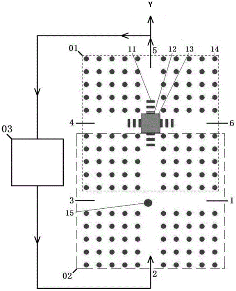
[0050] refer to figure 1 As shown, the lattice constant d=1 μm, the working wavelength is 2.976 μm, the radius of the circular high refractive index linear dielectric column 14 is 0.18 μm; the long side of the rectangular high refractive index linear dielectric column 11 is 0.613 μm, and the short side is 0.162 μm μm; the size of the rectangular high refractive index linear dielectric column 12 is consistent with the size of the rectangular high refractive index linear dielectric column 11; the side length of the square nonlinear dielectric column 13 is 1.5 μm, and the third-order nonlinear coefficient is 1.33*10 -2 μm 2 / V 2 The distance between two adjacent rectangular linear dielectric columns is 0.2668 μm; the radius of the circular nonlinear dielectric column 15 is 0.292 μm.

[0051] refer to figure 1 In the shown structure, port 1 and port 4 respectively input reference light E1 and E2, wherein E1=E2=1; when the output signal of signal output terminal 5 is transmitted...

Embodiment 2

[0053] In the same way, refer to figure 1 As shown, the lattice constant d=1 μm, the working wavelength is 2.976 μm, the radius of the circular high refractive index linear dielectric column 14 is 0.18 μm; the long side of the rectangular high refractive index linear dielectric column 11 is 0.613 μm, and the short side is 0.162 μm μm; the size of the rectangular high refractive index linear dielectric column 12 is consistent with the size of the rectangular high refractive index linear dielectric column 11; the side length of the square nonlinear dielectric column 13 is 1.5 μm, and the third-order nonlinear coefficient is 1.33*10 -2 μm 2 / V 2 The distance between two adjacent rectangular linear dielectric columns is 0.2668 μm; the radius of the circular nonlinear dielectric column 15 is 0.292 μm.

[0054] refer to figure 1 In the shown structure, port 1 and port 4 respectively input reference light E1 and E2, wherein E1=E2=1; when the output signal of signal output terminal...

Embodiment 3

[0056] refer to figure 1 As shown, the lattice constant d=0.5208 μm, the working wavelength is 1.55 μm, the radius of the circular high refractive index linear dielectric column 14 is 0.0937 μm; the long side of the rectangular high refractive index linear dielectric column 11 is 0.3193 μm, and the short side is 0.0844 μm; the size of the rectangular high refractive index linear dielectric column 12 is consistent with the size of the rectangular high refractive index linear dielectric column 11; the side length of the square nonlinear dielectric column 13 is 0.7812 μm, and the third-order nonlinear coefficient is 1.33*10 -2 μm 2 / V 2 The distance between two adjacent rectangular linear dielectric columns is 0.1389 μm; the radius of the circular nonlinear dielectric column 15 is 0.0937 μm.

[0057] refer to figure 1 In the shown structure, port 1 and port 4 respectively input reference light E1 and E2, wherein E1=E2=1; when the output signal of signal output terminal 5 is tr...


PUM

PropertyMeasurementUnit
radiusaaaaaaaaaa
radiusaaaaaaaaaa
refractive indexaaaaaaaaaa

Abstract

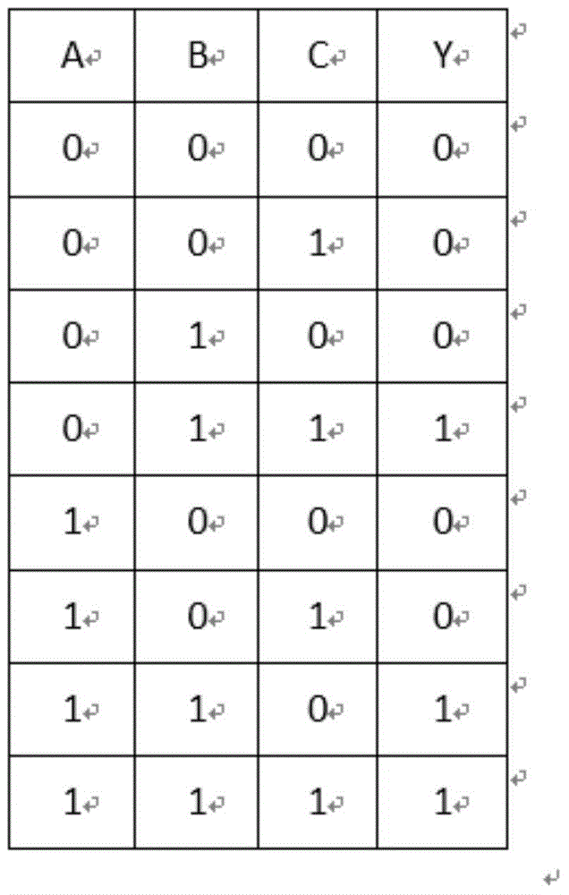
The invention discloses an optical clock generator. The optical clock generator comprises a nonlinear cavity unit, a cross-shaped waveguide logic gate unit and a time delayer unit. The optical clock generator is of a six-port photonic crystal structure and is composed of two reference light signal input ends, a feedback signal input end, a system signal and feedback signal output end and two idle ports. The output end of the cross-shaped waveguide logic gate unit is connected with the input end of the nonlinear cavity unit, the system signal output end of the nonlinear cavity unit is connected with the input end of the time delayer unit, the output end of the time delayer unit is connected with the input end of the cross-shaped waveguide logic gate unit, a signal output end is connected with a two-branch waveguide, one end of the two-branch waveguide serves as a system output port, the other end of the two-branch waveguide serves as a feedback signal output port connected to the input end of the time delayer unit, and the time delayer unit performs time delay on an input signal which is output to a feedback signal input end. The optical clock generator and other optical logic elements are easy to integrate.

Description

technical field [0001] The invention relates to a two-dimensional photonic crystal, nonlinear optics, and an optical clock generator. Background technique [0002] In 1987, E. Yablonovitch of Bell Laboratories in the United States was discussing how to suppress spontaneous emission, and S. John of Princeton University was discussing the photonic region and independently proposed the concept of photonic crystal (Photonic Crystal). A photonic crystal is a material structure in which dielectric materials are periodically arranged in space, and is usually an artificial crystal composed of two or more materials with different dielectric constants. [0003] With the introduction and in-depth research of photonic crystals, people can more flexibly and effectively control the movement of photons in photonic crystal materials. In combination with traditional semiconductor technology and integrated circuit technology, people are making rapid progress towards all-optical processing th...

Claims


Application Information

Patent Timeline
Patent Type & Authority Applications(China)
IPC IPC(8): G02F3/00G02B6/122
CPCG02F3/00G02B6/1225G02F1/3501G02F2201/06G02F2202/32
Inventor 欧阳征标余铨强
Owner SHENZHEN ZHIJIA LIFE NETWORK TECH CO LTD
Learn More