Method for increasing the switch ratio of graphene and nanowire heterojunction detector

A technology of heterojunction detectors and nanowires, applied in semiconductor devices, sustainable manufacturing/processing, electrical components, etc., can solve the problems of large dark current, low switching ratio, etc., to improve switching ratio, suppress dark current, Good believability and intuitive effect

Inactive Publication Date: 2015-04-22
SHANGHAI INST OF TECHNICAL PHYSICS - CHINESE ACAD OF SCI
View PDF0 Cites 6 Cited by
  • Summary
  • Abstract
  • Description
  • Claims
  • Application Information

AI Technical Summary

Problems solved by technology

But the bandgap of InAs nanowires is only 0.36eV, so InAs nanowire photodetectors have a large dark current and a very low on-off ratio

Method used


Image

  • Method for increasing the switch ratio of graphene and nanowire heterojunction detector
  • Method for increasing the switch ratio of graphene and nanowire heterojunction detector
  • Method for increasing the switch ratio of graphene and nanowire heterojunction detector

Examples


Embodiment Construction

[0017] The specific embodiment of the present invention is described in detail below in conjunction with accompanying drawing:

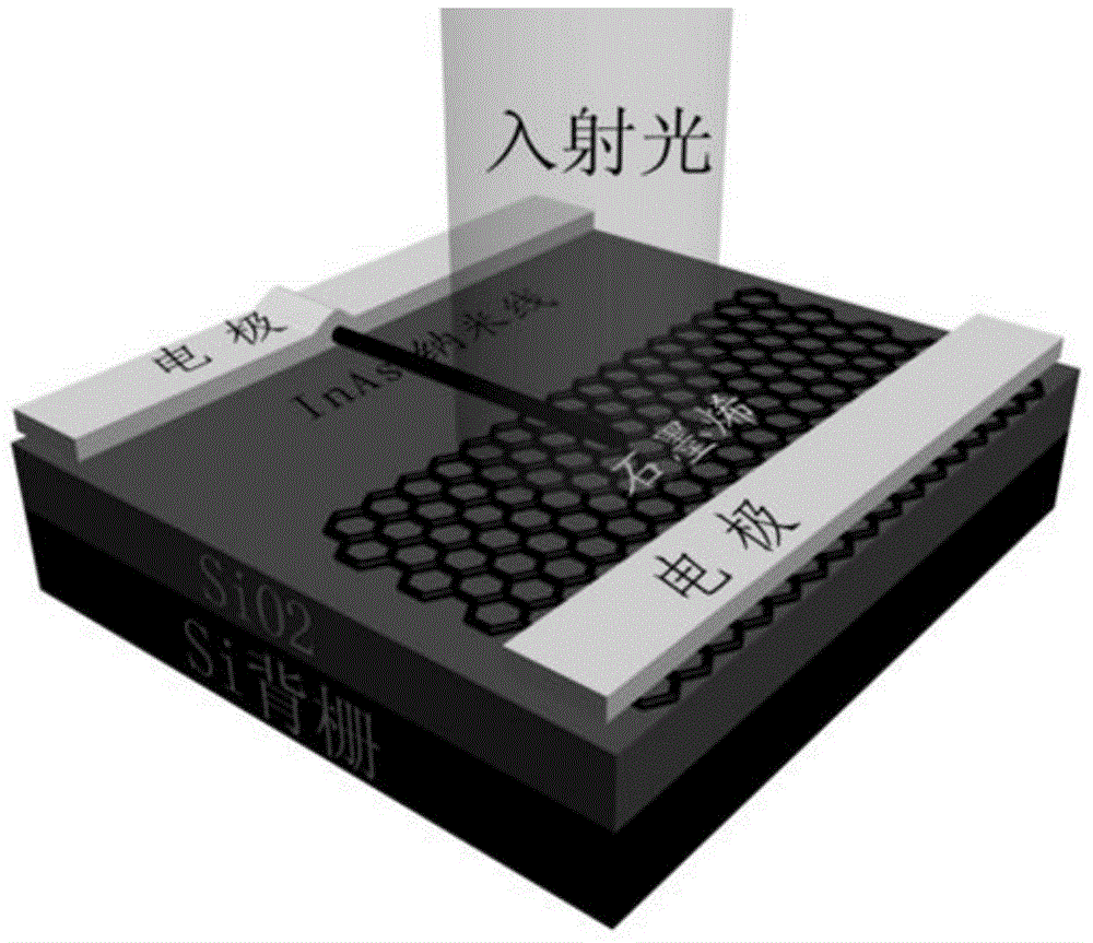
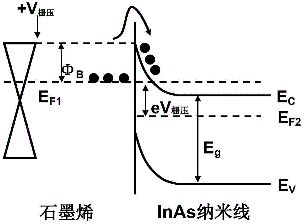
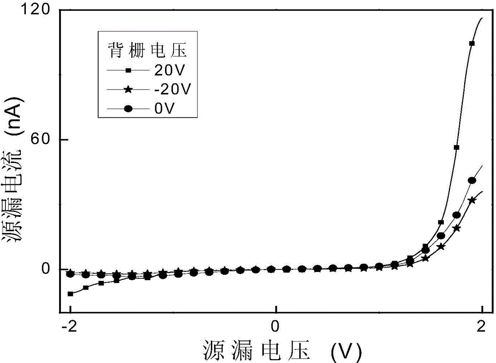
[0018] The present invention has developed graphene and InAs nanowire Schottky photodetectors, which have SiO 2 Single-layer graphene was prepared on the P-type Si substrate, and the epitaxially grown InAs nanowires were physically transferred to the single-layer graphene, and chromium and gold were deposited as source and drain electrodes by electron beam lithography and thermal evaporation technology.

[0019] Specific steps are as follows:

[0020] 1InAs nanowires are catalyzed by gold nanoparticles in the Riber 32MBE system, using vapor-liquid-solid (VLS) in GaAs(111) B growth on the substrate surface. First, the GaAs substrate is deoxidized at 630°C for 15 minutes, and a buffer layer of 300 nm is grown to obtain a relatively smooth surface. Then, transfer the GaAs substrate into the MBE preparation chamber, deposit an extremely thin gold film...


PUM

PropertyMeasurementUnit
lengthaaaaaaaaaa
diameteraaaaaaaaaa

Abstract

The invention discloses a method for increasing the switch ratio of a graphene and nanowire heterojunction detector. The method includes the steps that an InAs nanowire is transferred on mechanically-stripped graphene in a physical mode, and a heterojunction is formed; due to the fact that the graphene and the InAs nanowire have different work functions, a schottky barrier is formed at the contact position; the grid voltage can adjust the Fermi level of the graphene, the height of the schottky barrier can be adjusted accordingly, a built-in electric field is formed, photoproduction electron and hole pairs are separated quickly, electrons flow to the InAs nanowire, and holes flow to the graphene. Accordingly, the dark current of the graphene and nanowire heterojunction detector can be restrained effectively through the controllable advantages of the schottky barrier, and the switch ratio of the detector is increased; by means of the structure, the switch ratio of the graphene and the nanowire heterojunction detector can exceed 10<2>. The method has very great significance in increasing the switch ratio of the existing graphene and the nanowire heterojunction detector.

Description

technical field [0001] The invention relates to the design and testing of graphene and nanowire heterojunction detector structure, specifically refers to the use of the difference in the work function of graphene and InAs nanowires, the introduction of graphene and InAs nanowire Schottky barriers, the use of grid Regulating the Fermi level of graphene, thereby adjusting the height of the Schottky barrier, effectively suppressing the dark current of graphene and nanowire heterojunction detectors, and improving the on-off ratio. Background technique [0002] Graphene is a new material composed of a single layer of carbon atoms, in which the carbon atoms are sp 2 The hybrid orbitals form a two-dimensional structure of hexagonal honeycomb lattice. Graphene is currently the thinnest and hardest nanomaterial in the world, with extremely high electron mobility, so it is expected to be used to develop a new generation of electronic components or transistors that conduct electricity...

Claims


Application Information

Patent Timeline
Patent Type & Authority Applications(China)
IPC IPC(8): H01L31/18
CPCH01L31/108H01L31/18Y02P70/50
Inventor 胡伟达骆文锦王鹏苗金水郭楠陈平平李天信陈效双陆卫
Owner SHANGHAI INST OF TECHNICAL PHYSICS - CHINESE ACAD OF SCI
Why Eureka
Try Eureka