

Patterning etching method of transparent conducting electrode and patterning transparent conducting electrode
A transparent conductive electrode and patterning technology, which is applied to the conductive layer, circuit, and electrical components on the insulating carrier, can solve the problems of insufficient wettability between the etching solution and the protective layer, high requirements for equipment, and difficult cost control. Achieve the effects of improving electrode transparency, low cost, and low etching speed
- Summary
- Abstract
- Description
- Claims
- Application Information
AI Technical Summary
Problems solved by technology
Method used
Image

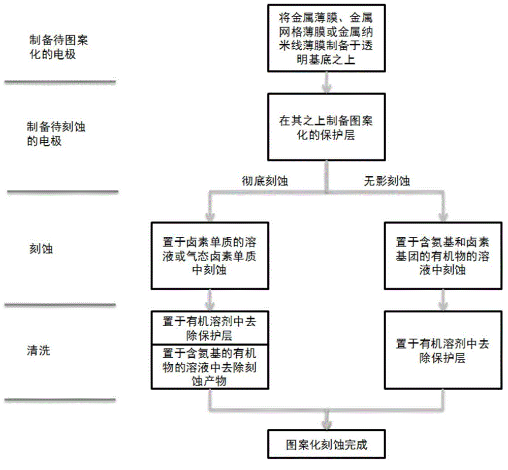
Examples
Embodiment 1
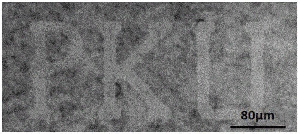
[0034] First, the aqueous dispersion of silver nanowires is scraped onto a glass substrate to form a thin film of silver nanowires, which is used as an electrode to be patterned. Then a commercial photoresist film was prepared on it by spin coating method, and a post-baking treatment was performed at 100° C. for 1.5 minutes to make an electrode to be exposed. After cooling, cover the mask plate with "PKU" pattern on it, and carry out ultraviolet exposure for 2 minutes to make the electrode to be developed. After completion, it was immersed in 1% NaOH aqueous solution for 10 seconds to develop, rinsed with water, and dried with nitrogen gas to prepare an electrode to be etched. After drying, put it into an iodine cylinder and seal it, let it react with gaseous iodine for 1 minute, take it out, wash off the photoresist in acetone, rinse it with water, and blow it dry with nitrogen. figure 2 It is an optical microscope photo of a silver nanowire sample patterned by a thorough e...
Embodiment 2
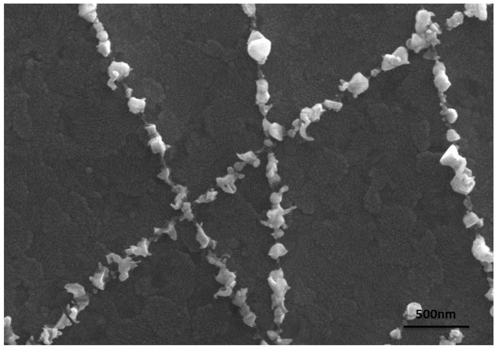
[0037]First, the isopropanol dispersion of silver nanowires was spin-coated on a glass substrate to form a thin film of silver nanowires, which was used as an electrode to be patterned. Then a commercial photoresist film was prepared on it by spin coating method, and a post-baking treatment was performed at 100° C. for 1.5 minutes to make an electrode to be exposed. After cooling, cover it with a mask plate and perform ultraviolet exposure for 2 minutes to make an electrode to be developed. After completion, it was immersed in 1% NaOH aqueous solution for 10 seconds to develop, rinsed with water, and dried with nitrogen gas to prepare an electrode to be etched. Then soak it in 1.2 mg / mL methylamine iodide (CH 3 NH 3 I) Etch in isopropanol solution for 5 minutes, rinse with water, and dry with nitrogen. After drying, the photoresist was washed off in acetone, rinsed with water, and dried with nitrogen. Finally, a transparent conductive electrode patterned by a shadowless et...
Embodiment 3
[0039] First, the isopropanol dispersion of silver nanowires is sprayed on a glass substrate to form a thin film of silver nanowires as an electrode to be patterned. Then, a commercial photoresist film was prepared on it by spin coating method, and a post-baking treatment was performed at 100° C. for 1.5 min to make an electrode to be exposed. After cooling, cover it with a mask plate with a grid pattern, and perform ultraviolet exposure for 2 minutes to make an electrode to be developed. After completion, it was immersed in 1% NaOH aqueous solution for 10 seconds to develop, rinsed with water, and dried with nitrogen gas to prepare an electrode to be etched. Then put it into an iodine tank and seal it, let it react with gaseous iodine for 1 minute, take it out, wash off the photoresist in acetone, rinse it with water, and dry it with nitrogen. Then immerse it in 20% amino-terminated polyether isopropanol solution for 30 seconds to remove the etching products, rinse it with c...
PUM
 Abstract
Description
Claims
Application Information