Processing method of deep etching smooth surface based on SiC substrate slice

A technology of smooth surface and processing technology, which is applied in the field of processing technology of wide bandgap semiconductor based on SiC substrate sheet deep etching smooth surface, can solve the problem that SiC is difficult to obtain smooth surface, etc., and achieve simple preparation method, controllable conditions and operation process concise effect

Inactive Publication Date: 2015-05-06
SHANGHAI NORMAL UNIVERSITY
View PDF6 Cites 5 Cited by
  • Summary
  • Abstract
  • Description
  • Claims
  • Application Information

AI Technical Summary

Problems solved by technology

[0004] The purpose of the present invention is to overcome the problem in the prior art that it is difficult to obtain a sm...

Method used


Image

  • Processing method of deep etching smooth surface based on SiC substrate slice
  • Processing method of deep etching smooth surface based on SiC substrate slice

Examples


Embodiment Construction

[0007] The present invention will be further described below in conjunction with the accompanying drawings and embodiments.

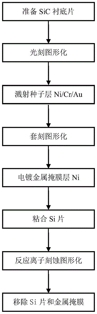
[0008] The present invention is based on the processing technology of deep etching smooth surface of SiC substrate (such as figure 1 shown), including the following steps:

[0009] Step 1, prepare the SiC substrate sheet: the substrate SiC substrate sheet is an ingot grown by the PVT method, which is oriented, cut, double-sided polished, and double-sided CMP polished to obtain a 3-inch industrial wafer, which is cut into 3×2cm 2 The substrates are cleaned by semiconductor RCA process.

[0010] Step 2, photolithographic patterning: place the substrate on a rubber drying table at 100°C for drying, and evenly spin-coat a 1 μm thick photoresist on the substrate through a coater, and place it on the rubber drying table for 5 minutes Pre-baking, then patterning it with a UV lithography machine, and hardening the film for 10 minutes after development.
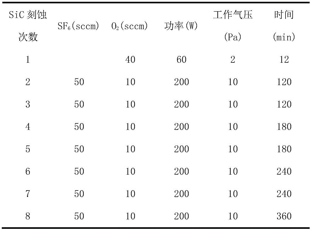
[00...


PUM

PropertyMeasurementUnit
Thicknessaaaaaaaaaa
Diameteraaaaaaaaaa
Thicknessaaaaaaaaaa

Abstract

The invention provides a processing method of deep etching a smooth surface based on a SiC substrate slice and relates to the technical field of deep etching of wide bandgap semiconductor materials. The processing method comprises the steps of cleaning the substrate, patterning the SiC substrate slice by virtue of the etched pattern transfer technology, forming a seed layer Ni/Cr/Au by virtue of ultrahigh vacuum magnetron sputtering to realize metal patterning, enhancing the electrical conductivity of the substrate by use of a seed layer, forming a micro-scale thick etching mask layer Ni by virtue of electroplating, gluing the substrate slice with a Si slice, forming a 72 microns deep circular strain film by virtue of RIE deep etching, removing the Si slice and the metal mask, and the like. The processing method has the characteristics of simple preparation method, simple operation process, controllable conditions and the like. Technical and material foundations are laid for the demand on high-temperature, high-power, high-frequency and low-loss devices having such characteristics of wide bandgap, high breakdown electric field, high electrical conductivity and high saturated electron drift velocity in the electronic industrial product market.

Description

technical field [0001] The invention relates to the technical field of deep etching processing of wide-bandgap semiconductors, and specifically refers to a processing technology for deep-etching smooth surfaces of wide-bandgap semiconductors with high mechanical hardness, good chemical stability and corrosion resistance based on SiC substrates. Background technique [0002] SiC material has now developed into one of the main wide bandgap semiconductor materials, with a variety of crystal forms, SiC has a wide bandgap (3.26eV), high breakdown electric field (2.3MV / cm), high thermal conductivity (4.9Wcm -1 K -1 ) and high saturation electron drift rate (2×10 7 cm / s) and other characteristics, and these characteristics are exactly what high temperature, high power, high frequency, low loss devices need, and it is also a very promising material for making micro devices under MEMS, especially in harsh environments devices for the following applications. Due to the high mechani...

Claims


Application Information

Patent Timeline
IPC IPC(8): H01L21/02
CPCH01L21/0475
Inventor 刘益宏赵高杰孙玉俊廖黎明程越刘少雄陈之战
Owner SHANGHAI NORMAL UNIVERSITY
Why Eureka
Try Eureka