
Heterostructure material with orderly transition of charge orbit and anisotropic field resistance effect and its preparation method and application

An anisotropic field and heterogeneous structure technology, applied in the manufacture/processing of electromagnetic devices, material selection, etc., can solve the problems of inability to control the charge orbit and non-magnetic field, disadvantages, etc.

Active Publication Date: 2017-11-07
INST OF PHYSICS - CHINESE ACAD OF SCI
View PDF4 Cites 0 Cited by
  • Summary
  • Abstract
  • Description
  • Claims
  • Application Information

AI Technical Summary

Problems solved by technology

However, the only currently available on SrTiO 3 Growth of Charge Orbital Ordered Nd on Single Crystal 0.5 Sr 0.5 MnO 3 and Pr 0.5 Sr 0.5 MnO 3 In the case of a thin film, it is impossible to effectively control the ordered phase of its charge orbit without a magnetic field, which is very unfavorable for practical applications.

Method used


Image

  • Heterostructure material with orderly transition of charge orbit and anisotropic field resistance effect and its preparation method and application
  • Heterostructure material with orderly transition of charge orbit and anisotropic field resistance effect and its preparation method and application
  • Heterostructure material with orderly transition of charge orbit and anisotropic field resistance effect and its preparation method and application

Examples


Embodiment 1

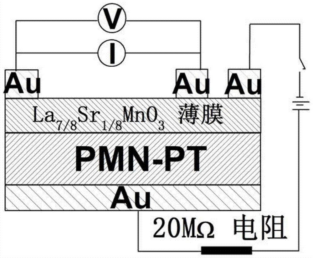
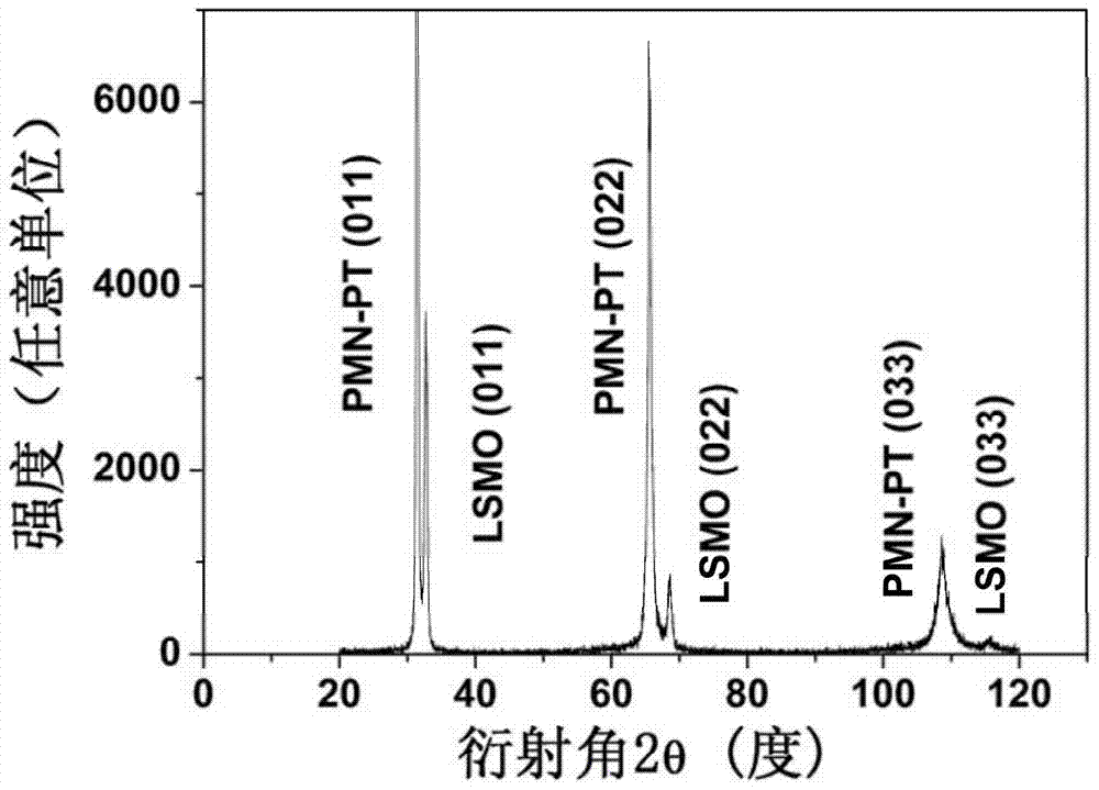
[0039] In this embodiment, PMN-PT (0.7Pb(Mg) of (011) orientation 1 / 3 Nb 2 / 3 )O 3 -0.3PbTiO 3 ) La on a single crystal substrate with a thickness of 30 nm 7 / 8 Sr 1 / 8 MnO 3 In the thin film, a large in-plane anisotropic tensile strain is introduced, orderly transformation of the charge orbit is observed, and the resistance is greatly reduced by an external bias electric field, and a large anisotropic field-induced resistance effect appears.

[0040] Concrete preparation method is as follows:

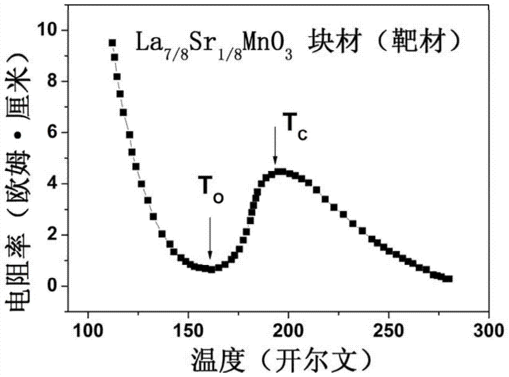
[0041] (1) Preparation of perovskite-type manganese oxide target: La 2 o 3 (purity: 99.99%), SrCO 3 (purity: 99.9%) and MnCO 3 (Purity: 99.9%) According to the chemical formula La 7 / 8 Sr 1 / 8 MnO 3 The stoichiometric ratio for batching. Grind the prepared raw materials thoroughly to make them evenly mixed. Then put it in a muffle furnace and pre-fire it for the first time at 900°C for 12 hours to completely decompose the carbonate. The obtained product was fully ground and c...


PUM

PropertyMeasurementUnit
thicknessaaaaaaaaaa
thicknessaaaaaaaaaa

Abstract

The present invention provides a heterogeneous structure material with ordered characteristics of charge orbits and anisotropic field resistance effect. The heterostructure material comprises: (011) or its obliquely oriented PMN-PT single crystal substrate and A perovskite manganese oxide thin film epitaxially grown thereon, wherein the lattice mismatch between the substrate and the thin film is 1-6%. The invention realizes orderly transition of electric charge track in the thin film by introducing large anisotropic tensile strain in the plane. The orderly arrangement of the formed charge orbits is sensitive to the applied bias electric field, which shows that the film resistance under the action of the bias electric field drops significantly, and the low temperature region produces a large anisotropic field resistance effect higher than the magnetoresistance. By controlling the film thickness, The magnitude and polarity of the bias electric field can easily adjust the magnitude of the field resistance to meet the needs of practical applications. The heterostructure material has the characteristics of simple preparation process, low power consumption, convenient and easy operation, etc., which is beneficial to device development and application.

Description

technical field [0001] The invention relates to a perovskite manganese oxide film with a charge orbit order and a large anisotropic field induced by growing a (011) oriented perovskite manganese oxide film on a relaxed ferroelectric single crystal substrate (PMN-PT). Heterostructure material with resistance effect and its preparation method and use. Background technique [0002] Based on the strong coupling between multiple degrees of freedom such as charge, orbit, spin and lattice, ABO 3 type perovskite type manganese oxide Re 1-x Ae x MnO 3 (Re=La, Ce, Pr, etc., Ae=Ca, Sr, Ba, etc.) have complex electromagnetic and structural phase diagrams and various interesting physical phenomena, such as giant magnetoresistance effects, charge, spin, and orbital ordering phenomena , Jahn-Teller distortion, metal-insulator phase transition, phase separation, etc., involve many basic problems in condensed matter physics. The ordering of charge orbitals is one of the most interesting...

Claims


Application Information

Patent Timeline
Patent Type & Authority Patents(China)
IPC IPC(8): H01L43/10H01L43/12H10N50/01
Inventor 王晶胡凤霞赵莹莹匡皓卢海霞孙继荣沈保根
Owner INST OF PHYSICS - CHINESE ACAD OF SCI
Learn More