

Mask read only memory and manufacturing method thereof
A read-only memory and model technology, which is applied in the manufacture of mask read-only memory and the field of mask read-only memory, can solve the problems of reducing device integration, increasing device area, and small array area, so as to reduce leakage and isolation effects Good, the effect of reducing the area
- Summary
- Abstract
- Description
- Claims
- Application Information
AI Technical Summary
Problems solved by technology
Method used
Image

Examples
Embodiment Construction
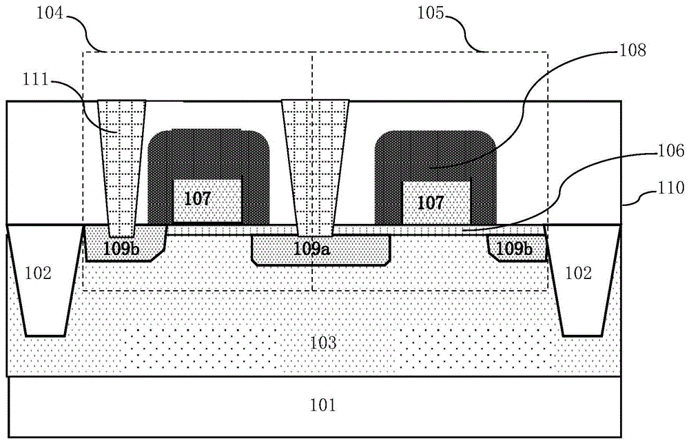
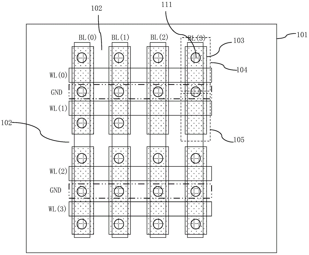
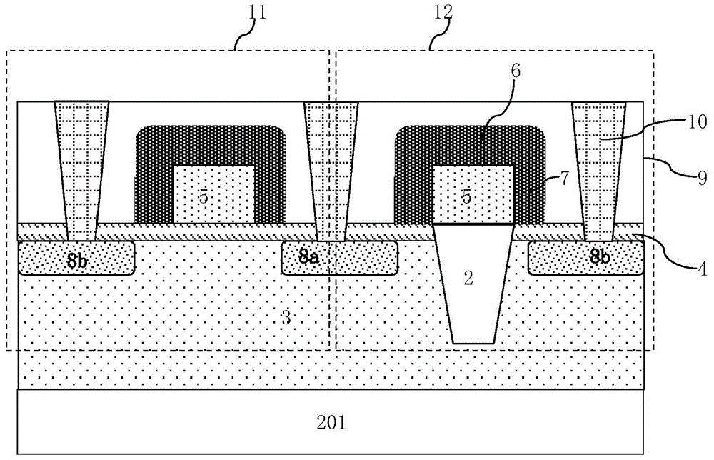
[0047] Such as image 3 Shown is the cross-sectional view of the NMOS storage unit of the mask type ROM in the embodiment of the present invention; as Figure 4 Shown is the layout of the mask ROM according to the embodiment of the present invention. In the embodiment of the present invention, the mask read-only memory is formed on a silicon substrate 201, and a shallow trench field oxygen 2 isolation structure is formed on the silicon substrate 201, and a plurality of active Area 3: The array structure of the mask read-only memory includes a plurality of vertically arranged bit lines BL, a plurality of horizontally arranged word lines WL, and a plurality of horizontally arranged ground lines GND; Figure 4 The CCP shows 8 bit lines BL, namely BL(0), BL(1), BL(2), BL(3), BL(4), BL(5), BL(6) and BL(7), Seven bit lines WL are WL(0), WL(1), WL(2), WL(3), WL(4), WL(5) and WL(6), and four ground lines GND.
[0048] Below each of the bit lines BL corresponds to one or more of the...
PUM
 Abstract
Description
Claims
Application Information