Manufacturing method of light emitting diode epitaxial wafer
A technology of light-emitting diodes and manufacturing methods, which is applied to electrical components, circuits, semiconductor devices, etc., can solve problems such as poor crystal quality and poor antistatic ability, and achieve improved crystal quality, improved antistatic ability, and ease of concave deformation. Effect
- Summary
- Abstract
- Description
- Claims
- Application Information
AI Technical Summary
Problems solved by technology
Method used
Image
Examples
Embodiment 1
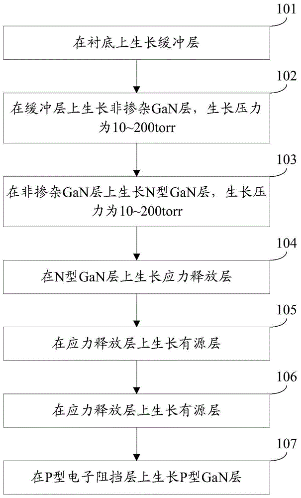
[0027] The embodiment of the present invention provides a method for manufacturing a light-emitting diode epitaxial wafer, which is especially suitable for large-scale epitaxial wafers of 4 inches, 6 inches, and 8 inches. See figure 1 , the manufacturing method includes:
[0028] Step 101: growing a buffer layer on a substrate.
[0029] Specifically, the substrate may be a sapphire substrate.
[0030] In practical application, Metal-Organic Chemical Vapor Deposition (MOCVD) method can be used, trimethyl (or triethyl) gallium is used as gallium source, high-purity NH3 is used as nitrogen source, trimethyl Base indium is used as the indium source, trimethylaluminum is used as the aluminum source, silane is selected for n-type doping, and magnesocene is selected for p-type doping to realize the manufacturing method of the light-emitting diode epitaxial wafer provided in this embodiment.
[0031] Step 102: growing a non-doped GaN layer on the buffer layer with a growth pressure ...
Embodiment 2
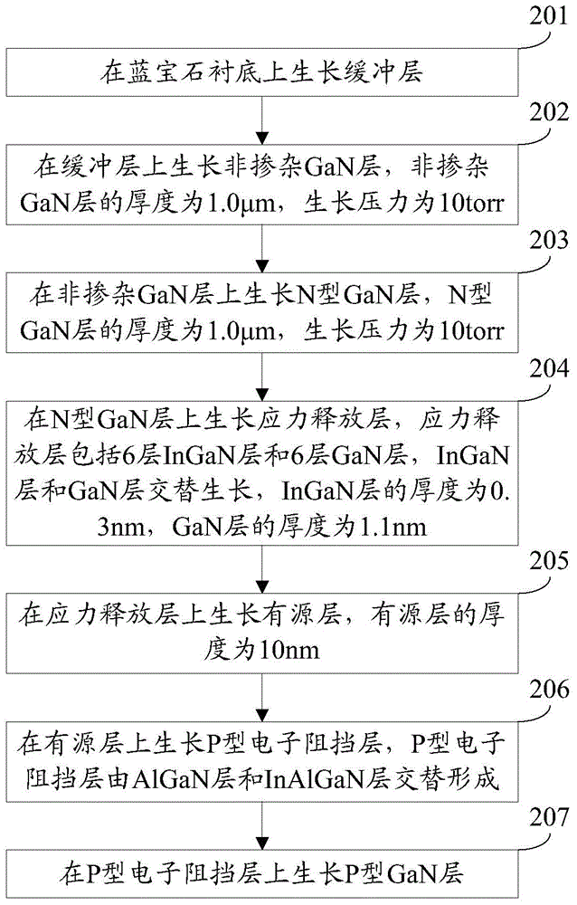
[0069] An embodiment of the present invention provides a method for manufacturing a light-emitting diode epitaxial wafer. This embodiment is a specific implementation of the method for manufacturing a light-emitting diode epitaxial wafer provided in Embodiment 1. Refer to figure 2 , the manufacturing method includes:
[0070] Step 201: growing a buffer layer on a sapphire substrate.
[0071] Step 202: growing a non-doped GaN layer on the buffer layer, the thickness of the non-doped GaN layer is 1.0 μm, and the growth pressure is 10 torr.
[0072] Specifically, the growth rate of the non-doped GaN layer is 2.0 μm / h, and when growing the non-doped GaN layer, the growth rate of the non-doped GaN layer remains unchanged. The flow rate of the Ga source is 200-500 sccm, and when the non-doped GaN layer is grown, the flow rate of the Ga source gradually increases.
[0073] Step 203: growing an N-type GaN layer on the non-doped GaN layer, the thickness of the N-type GaN layer is 1....
PUM
| Property | Measurement | Unit |
|---|---|---|
| Thickness | aaaaa | aaaaa |
| Thickness | aaaaa | aaaaa |
| Thickness | aaaaa | aaaaa |
Abstract
Description
Claims
Application Information

