A method of manufacturing a light-emitting diode epitaxial wafer
A technology of light-emitting diodes and manufacturing methods, applied in electrical components, circuits, semiconductor devices, etc., can solve the problems of poor crystal quality and poor anti-static ability, and achieve the effects of improving crystal quality, improving anti-static ability and reducing temperature difference
- Summary
- Abstract
- Description
- Claims
- Application Information
AI Technical Summary
Problems solved by technology
Method used
Image
Examples
Embodiment 1
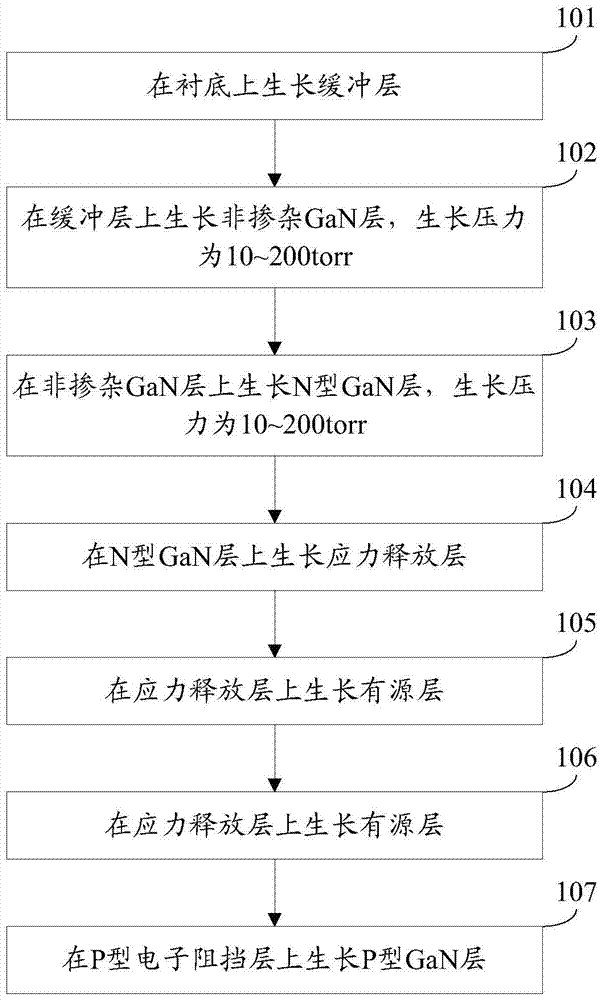
[0026] The embodiment of the present invention provides a method for manufacturing a light-emitting diode epitaxial wafer, which is especially suitable for large-scale epitaxial wafers of 4 inches, 6 inches, and 8 inches. See figure 1 , the manufacturing method includes:
[0027] Step 101: growing a buffer layer on a substrate.
[0028] Specifically, the substrate may be a sapphire substrate.
[0029] In practical application, Metal-Organic Chemical Vapor Deposition (MOCVD) method can be used, with trimethyl (or triethyl) gallium as gallium source, high-purity NH3 as nitrogen source, trimethyl Indium is used as an indium source, trimethylaluminum is used as an aluminum source, silane is selected for n-type doping, and magnesocene is selected for p-type doping to realize the manufacturing method of a light-emitting diode epitaxial wafer provided in this embodiment.
[0030] Step 102: growing a non-doped GaN layer on the buffer layer with a growth pressure of 10-200 torr.
[...
Embodiment 2
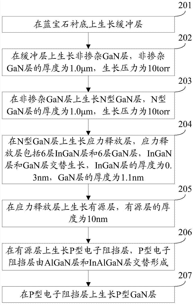
[0068] An embodiment of the present invention provides a method for manufacturing a light-emitting diode epitaxial wafer. This embodiment is a specific implementation of the method for manufacturing a light-emitting diode epitaxial wafer provided in Embodiment 1. Refer to figure 2 , the manufacturing method includes:
[0069] Step 201: growing a buffer layer on a sapphire substrate.
[0070] Step 202: growing a non-doped GaN layer on the buffer layer, the thickness of the non-doped GaN layer is 1.0 μm, and the growth pressure is 10 torr.
[0071] Specifically, the growth rate of the non-doped GaN layer is 2.0 μm / h, and when growing the non-doped GaN layer, the growth rate of the non-doped GaN layer remains unchanged. The flow rate of the Ga source is 200-500 sccm, and when the non-doped GaN layer is grown, the flow rate of the Ga source gradually increases.
[0072] Step 203: growing an N-type GaN layer on the non-doped GaN layer, the thickness of the N-type GaN layer is 1....
PUM
 Abstract
Description
Claims
Application Information
 - R&D
- Intellectual Property
- Life Sciences
- Materials
- Tech Scout
- Unparalleled Data Quality
- Higher Quality Content
- 60% Fewer Hallucinations
Browse by: Latest US Patents, China's latest patents, Technical Efficacy Thesaurus, Application Domain, Technology Topic, Popular Technical Reports.
© 2025 PatSnap. All rights reserved.Legal|Privacy policy|Modern Slavery Act Transparency Statement|Sitemap|About US| Contact US: help@patsnap.com


