

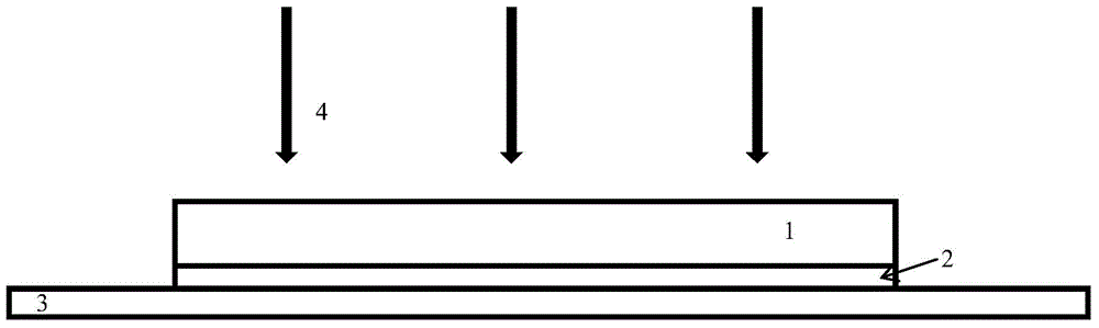
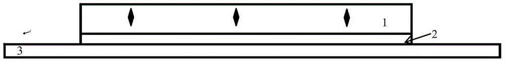
Method for cutting wafer of high-power power electronic device by invisible laser
A power electronic device, laser cutting technology, applied in the direction of laser welding equipment, welding equipment, metal processing, etc., can solve the problems of chip surface damage, cracking, damage chip reliability, etc., to achieve reliability assurance and good reliability Effect
- Summary
- Abstract
- Description
- Claims
- Application Information
AI Technical Summary
Problems solved by technology
Method used
Image


Examples
Embodiment 1
[0047] Under the guidance of the cutting principle provided by the present invention, the specific implementation parameters selected: the laser beam wavelength is 190nm, the cutting groove depth is 20 μm, the laser beam power is 5W, the focusing distance is 50 μm, and the laser cutting speed is 10mm / s.
Embodiment 2
[0049] Under the guidance of the cutting principle provided by the present invention, the parameters are selected specifically: the laser beam wavelength is 300nm, the cutting groove depth is 40μm, the laser beam power is 10W, the focusing distance is 80μm, and the laser cutting speed is 10mm / s.
Embodiment 3
[0051] Under the guidance of the cutting principle provided by the present invention, specific implementation parameter selection: laser beam wavelength 220nm, cutting groove depth 20μm, laser beam power 8W, focusing distance 100μm, laser cutting speed 150mm / s.
PUM
| Property | Measurement | Unit |
|---|---|---|
| wavelength | aaaaa | aaaaa |
| wavelength | aaaaa | aaaaa |
| power | aaaaa | aaaaa |
Abstract
Description
Claims
Application Information