A flash memory device and programming method thereof

A flash memory device and substrate technology, applied in static memory, read-only memory, instruments, etc., can solve the problems of flash memory device upgrade and key size reduction, large depletion layer width, device punch-through, etc., to achieve resistance to threshold voltage drift, Increased cell density, reduced readout errors

Active Publication Date: 2019-02-19
SHANGHAI HUALI MICROELECTRONICS CORP
View PDF6 Cites 0 Cited by
  • Summary
  • Abstract
  • Description
  • Claims
  • Application Information

AI Technical Summary

Problems solved by technology

[0005] However, there is another problem in the technical solution in the above-mentioned patent: because the voltage applied to the drain terminal is relatively high, the width of the depletion layer extending from the drain terminal to the substrate is relatively large, and the source terminal and the depletion region are easily exposed to high voltage. The bottom contacts together, resulting in device punchthrough and failure, that is, channel punchthrough effect (Channel punchthrough effect), which is a phenomenon in which the depletion region of the source end and the drain end are connected. This defect often limits the process of flash memory devices. Upgrading of technology nodes and shrinking of critical dimensions

Method used


Image

  • A flash memory device and programming method thereof
  • A flash memory device and programming method thereof

Examples


Embodiment 1

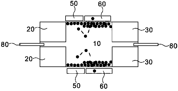
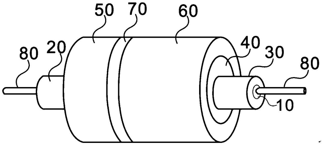
[0026] In this implementation, the control gate 50 and the floating gate 60 are made of polysilicon, the control gate 50 has a length of 10nm and a height of 90nm, and the floating gate 60 has a height of 70nm and a length of 40nm; the first insulating layer 40 and the second insulating layer 70 are made of two Silicon oxide, the thickness of the first insulating layer 40 is 2.5 nm, and the length of the second insulating layer 70 is 3 nm. The manufacturing process of the device can be selected from the top-down technology compatible with the standard CMOS process.

[0027] The flash memory memory provided by the present invention adopts a cylindrical substrate structure, on which the gate is covered, and the ends are led out through contact wires for applying substrate voltage. Compared with the prior art, the use of a cylindrical structure can enable the voltage of the control gate and the floating gate to better control the channel, reduce the percentage of the total deplet...

Embodiment 2

[0030] The voltage value applied to the control gate 50 is equal to the threshold voltage value of the flash memory device, the voltage value applied to the floating gate 60 is twice the threshold voltage value of the flash memory device, the voltage applied to the drain terminal 30 is 4V, and the voltage applied to the substrate 10 is 5V. A voltage of 0V is applied to the source terminal 20 .

[0031] The compiling principle of the present invention is: the voltage value applied to the control gate 50 is equal to the threshold voltage value of the flash memory device, and a thinner channel electron layer is induced in the lower substrate region. The voltage applied to the floating gate 60 is twice the threshold voltage of the flash memory device, and a thicker channel electron layer is induced in the lower channel electron layer. A high voltage is applied to the substrate 10 to accelerate the electrons in the thinner channel electron layer, generate hot electrons with suffici...


PUM


Abstract

The invention provides a flash memory device and a programming method thereof. The flash memory device comprises a substrate, wherein the substrate is of a cylindrical structure; a source end and a drain end are respectively arranged at the end parts of the substrate; a grid is coats the middle of the substrate; a first insulating layer is arranged between the grid and the substrate; the grid comprises a control grid and a floating grid parallel to each other; and contact lines are respectively led out of the two ends and are used for applying voltage to the substrate. According to the programming method of the flash memory device, by utilizing a back grid bias assisted hot electron generating mechanism, low voltage can be applied to the drain end, the key size of a split floating grid flash memory is effectively shortened, and the cell density of a flash memory array is increased, namely the memory capacity and density of the flash memory are increased. The movement of hot electrons is assisted by applying bias voltage, enough energy crossing an oxide layer is provided so as to finish compiling, the compiling efficiency of the flash memory is improved, and the compiling current power consumption is reduced.

Description

technical field [0001] The invention relates to the field of semiconductor integrated circuits and its manufacture, in particular to a flash memory device and its programming method. Background technique [0002] In semiconductor storage devices, flash memory is a non-volatile memory, and belongs to erasable programmable read-only memory (EPROM). Generally, a flash memory has two gates (a floating gate and a control gate), wherein the floating gate is used to store charges, and the control gate is used to control data input and output. The position of the floating gate is below the control gate, and it is in a floating state because it is not connected to the external circuit. The advantage of flash memory is that it can erase the entire memory block, and the erasing speed is fast, only about 1 to 2 seconds. Generally speaking, flash memory has a split gate structure or a stacked gate structure or a combination of the two structures. Due to its special structure, split-ga...

Claims


Application Information

Patent Timeline
Patent Type & Authority Patents(China)
IPC IPC(8): G11C16/10G11C16/34
Inventor 顾经纶
Owner SHANGHAI HUALI MICROELECTRONICS CORP
Why Eureka
Try Eureka