Quantum well structure of photoelectric device

A photoelectric device and quantum well technology, which is applied in the field of quantum well structure, can solve the problems that holes cannot be injected effectively, hole migration rate is blocked, and electrons in the N layer are easy to migrate, so as to achieve quantum confinement with weakened Stark effect and electron Effects of improved blocking efficiency and increased hole injection efficiency

Inactive Publication Date: 2015-05-20
西安利科光电科技有限公司
View PDF3 Cites 10 Cited by
  • Summary
  • Abstract
  • Description
  • Claims
  • Application Information

AI Technical Summary

Problems solved by technology

[0004] But at the same time, due to the reduction of the barrier height, the electrons in the N layer will easily migrate to the P layer and reduce the efficiency. If Al is added to the quantum barrier, the barrier layer can effectively block the electrons migrating to the P layer to improve efficiency, but

Method used


Image

  • Quantum well structure of photoelectric device
  • Quantum well structure of photoelectric device
  • Quantum well structure of photoelectric device

Examples


Embodiment 1

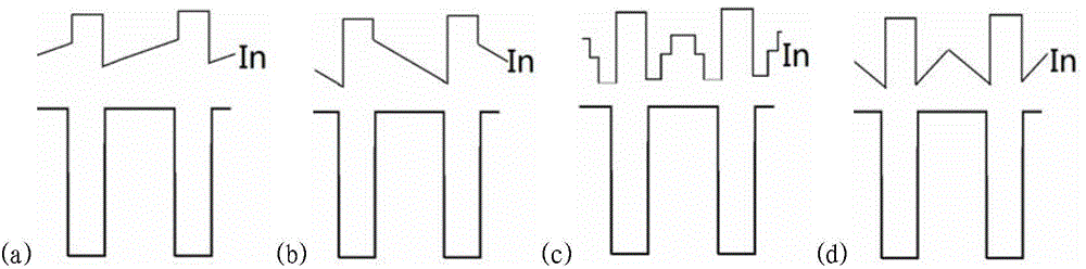
[0027] Low power high brightness chip design under low current. Can be designed as figure 1 In the structure shown in (a), the distribution of In components in each barrier layer increases linearly and gradually, and the proportion of In in the barrier layer gradually changes from X to Y, where X is 0.1% and Y is 5%.

[0028] It has been verified that the brightness of the structure adopting the gradual change of the In composition of the barrier layer is 20%-30% higher than that of the traditional structure.

Embodiment 2

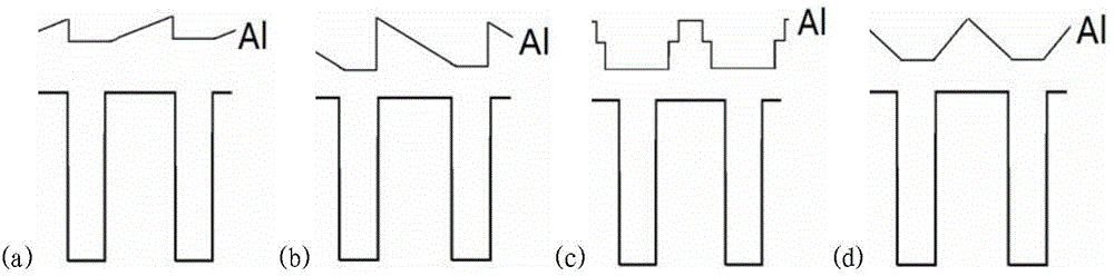
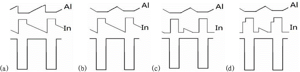
[0030] Low power high brightness chip design under high current. All barriers can be designed as figure 1 The structure shown in (a) combined with the design of the Al composition of the last two barrier layers is designed as figure 2 (a), the distribution of In components in each barrier layer increases linearly and gradually, and the proportion of In in this barrier layer gradually changes from X to Y, where X is 0.1%, Y is 5%, and the last two barrier layers The distribution of the inner Al component increases linearly and gradually, and the proportion of the Al component in the barrier layer changes gradually from M to N, where M is 0.1% and N is 5%.

[0031] It has been verified that the brightness of the structure using the gradual change of the In composition of the barrier layer combined with the gradual change of the Al composition of the last two barrier layers is 13% higher than that of the traditional structure, and the maximum current value that can be passed is...

Embodiment 3

[0033] The design of medium power and high brightness chip under high current. All barriers can be designed as figure 1 The structure shown in (a) combined with the design of the Al composition except the last 2 barrier layers is designed as figure 2 (c), the Al composition of the last two barrier layers is designed as figure 2 (d), the distribution of In components in each barrier layer increases linearly and gradually, and the proportion of In in this barrier layer gradually changes from X to Y, where X is 0.1%, and Y is 5%; except the last two barriers The Al composition outside the layer gradually changes in a trapezoidal manner, the Al content of the high Al composition position is 3.5%, and the Al content of the low Al composition position is 1.5%; the distribution of the Al composition in the last two barrier layers increases linearly and gradually. The proportion of Al components in the layer is gradually changed from M to N, where M is 0.1% and N is 3.5%.

[0034...


PUM


Abstract

The invention provides a new quantum well structure, which can further effectively increase the recombination probability of carrier, improve quantum efficiency and realize optimization and improvement of efficiency of a photoelectric device. AlInGaN is used as a barrier, an In and Al component gradual barrier layer structure is designed to substitute barrier layer structure design of the conventional quantum well structure. The In component is doped into the barrier layer structure of the quantum well, the band bending of the quantum well is reduced, a quantum confined stark effect is weakened, the electron blocking efficiency of an electron barrier layer is improved, a hole injection efficiency of the quantum well is increased, spatial wave function overlap of electrons and space is increased, and these have a positive effect on improvement of luminous efficiency of an LED (Light Emitting Diode); meanwhile the Al component is doped into the barrier layer structure of the quantum well, so migration of the electrons to a P layer is effectively blocked; through the gradual component design of the AlInGaN, the influence of a polarization electric field can be reduced, and the spontaneous emission spectrum strength of the quantum well is improved.

Description

Technical field: [0001] The invention belongs to the technical field of photoelectric device design and relates to a quantum well structure of a photoelectric device. Background technique: [0002] The quantum well structure design in the prior art is basically an alternating structure of quantum barriers and quantum wells, in which the material component band gap of the quantum barrier is larger than the material component band gap of the quantum well, and electrons and holes pass through under the action of an external electric field. Recombination luminescence occurs when the barrier layer reaches the well layer. In the traditional quantum well structure, the quantum well is composed of 1-3nm thick InGaN material. The concentration of In component determines the wavelength of the light-emitting device. The quantum barrier is composed of 6nm-15nm GaN material. The quantum well can trap carriers. And improve the luminous efficiency. Due to the existence of the polarizatio...

Claims


Application Information

Patent Timeline
IPC IPC(8): H01L33/06
Inventor 李淼
Owner 西安利科光电科技有限公司
Why Eureka
Try Eureka