Organic light emitting device and manufacturing method thereof

An electroluminescent device and luminescent technology, which is applied in the direction of electric solid-state devices, semiconductor/solid-state device manufacturing, electrical components, etc., can solve the problem of low luminous efficiency

Inactive Publication Date: 2015-05-20
OCEANS KING LIGHTING SCI&TECH CO LTD +2
View PDF0 Cites 0 Cited by
  • Summary
  • Abstract
  • Description
  • Claims
  • Application Information

AI Technical Summary

Problems solved by technology

However, the luminous efficiency of organic electroluminescent devices is low at present

Method used


Image

  • Organic light emitting device and manufacturing method thereof
  • Organic light emitting device and manufacturing method thereof
  • Organic light emitting device and manufacturing method thereof

Examples


preparation example Construction

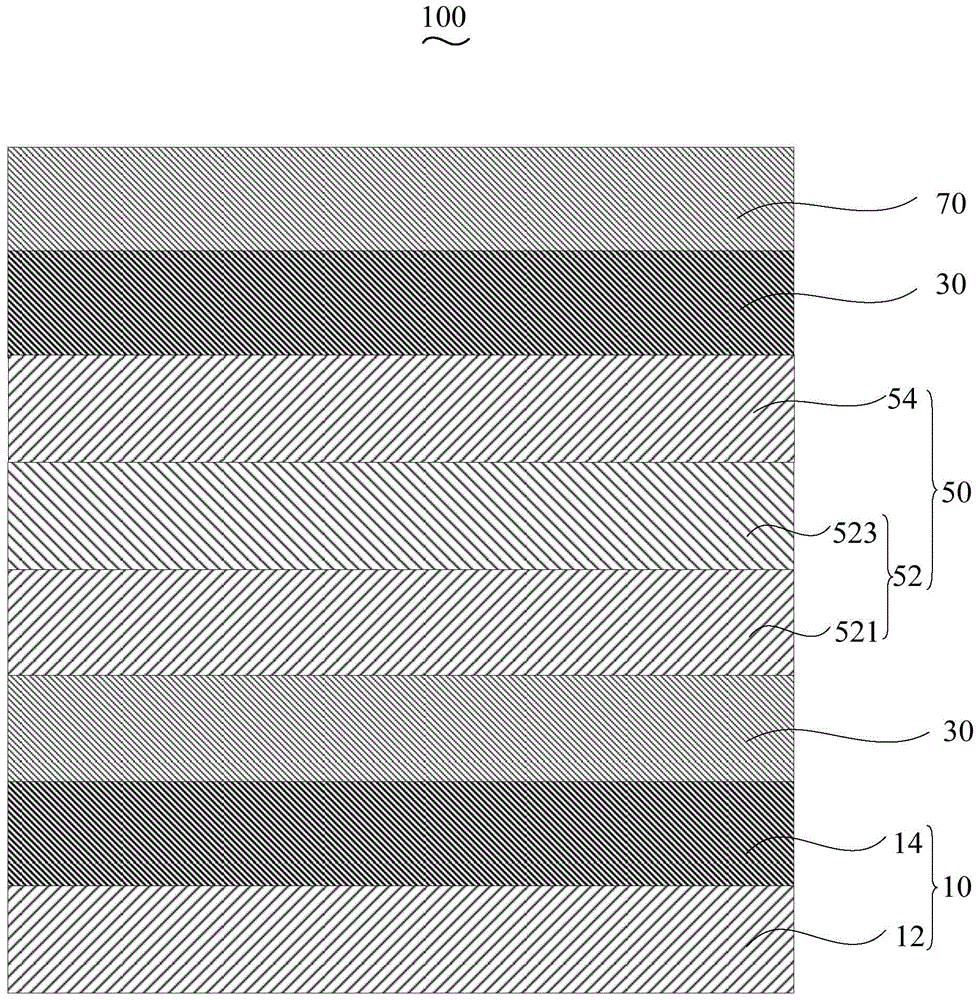
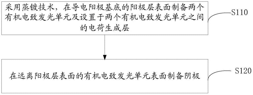
[0042] Please also see figure 2 , the preparation method of the organic electroluminescent device 100 of one embodiment, it comprises the following steps:

[0043] Step S110 , preparing two organic electroluminescent units 30 and a charge generation layer 50 disposed between the two organic electroluminescent units 30 on the surface of the anode layer 14 of the conductive anode substrate 10 using evaporation technology.

[0044] The conductive anode substrate 10 includes a transparent substrate 12 and an anode layer 14 prepared on the transparent substrate 12 . Preferably, the transparent substrate 12 is glass. The material of the anode layer 14 is indium tin oxide (ITO). The sheet resistance of the anode layer 14 is 5-100Ω / sq.

[0045] Preferably, before the conductive anode substrate 10 is used, a step of cleaning the conductive anode substrate 10 is also included. The cleaning steps are as follows: the base of the conductive anode is ultrasonically cleaned with deterge...
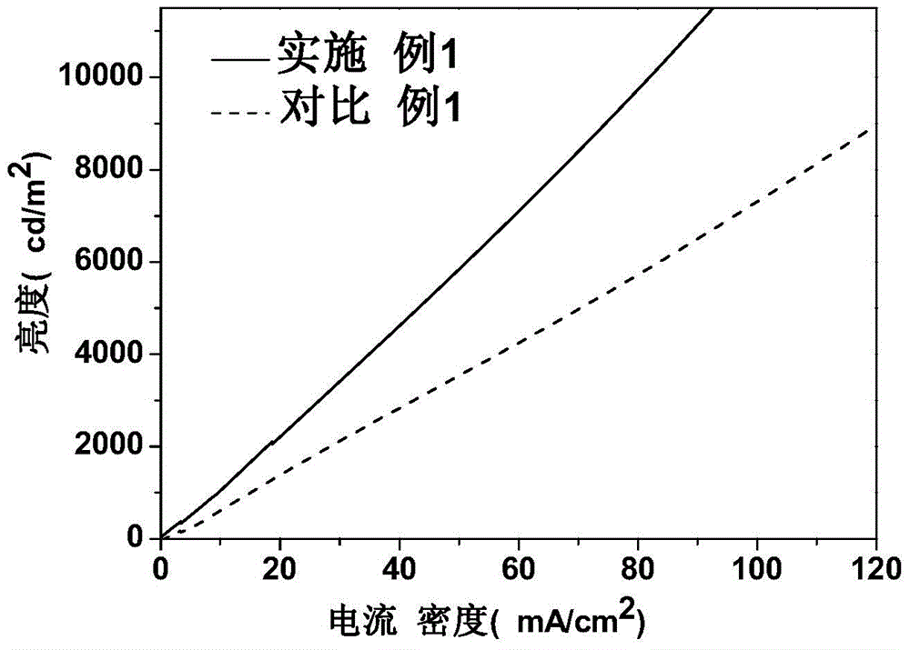
Embodiment 1

[0075] The structure prepared in this example is ITO glass / NPB / NPB: Ir(MDQ)2(acac) / Bphen / Li 2 CO 3 : Organic electroluminescent device of Bphen / ZnO / HAT-CN / m-MTDATA / CBP: FIr6 / Bphen / Mg-Al. Among them, the slash " / " indicates a layered structure, and the colon ":" indicates doping, the same below.

[0076] The preparation of the organic electroluminescent device of this embodiment comprises the following steps:

[0077] The conductive substrate is provided as the anode, and cleaned, it is ITO conductive glass, and the sheet resistance is 5Ω / □.

[0078] In a vacuum of 1 x 10- 5 In Pa's vacuum coating system, a hole transport layer is prepared on the surface of the ITO conductive film, the material is NPB, the thickness is 20nm, and the evaporation rate of NPB is 0.1nm / s.

[0079] In a vacuum of 1×10 -5 In the vacuum coating system of Pa, the light-emitting layer is prepared on the surface of the hole transport layer by thermal resistance evaporation technology, and the materi...

Embodiment 2

[0089] The structure prepared in this example is ITO glass / MeO-TPD / DCJTB:Alq3 / TPBi / Cs 2 CO 3 : TPBi / SnO 2 / HAT-CN / MeO-TPD / DPVBi / TPBi / Al organic electroluminescent devices.

[0090] The preparation of the organic electroluminescent device of this embodiment comprises the following steps:

[0091] The conductive substrate is provided as the anode, and cleaned, it is ITO conductive glass, and the sheet resistance is 100Ω / □.

[0092] In a vacuum of 1 x 10- 3 In the vacuum coating system of Pa, a hole transport layer is prepared on the surface of the ITO film, the material is MeO-TPD, the thickness is 80nm, and the evaporation rate of MeO-TPD is 1nm / s.

[0093] In a vacuum of 1 x 10- 3 In the vacuum coating system of Pa, the light-emitting layer is prepared on the surface of the hole transport layer by thermal resistance evaporation technology. The material of the light-emitting layer is a mixture of DCJTB and Alq3. The mass ratio of DCJTB to Alq3 is 5:100. The evaporation rat...


PUM


Abstract

An organic light emitting device comprises a conductive anode substrate, a cathode, an anode layer, at least two organic light emitting units and charge generating layers, wherein the organic light emitting units are stacked between the anode layer of the conductive anode substrate and the cathode, and the charge generating layers are arranged between the adjacent organic light emitting units. Each charge generating layer comprises an n-type layer and a p-type layer which are stacked, the n-type layer is adjacent to the anode layer and comprises an organic doping layer and an inorganic layer which are stacked sequentially, the p-type layer is adjacent to the cathode and is stacked on the surface of an inorganic layer. The inorganic layer is made of zinc oxide, ceric oxide or stannic oxide, the organic doping layer is composed of host materials and dopant doped in the host materials. The organic light emitting device is high in light emitting efficiency. The invention further provides a manufacturing method of the organic light emitting device.

Description

technical field [0001] The invention relates to an organic electroluminescence device and a preparation method thereof. Background technique [0002] The luminescence principle of organic electroluminescent devices is based on the action of an external electric field, electrons are injected from the cathode to the lowest unoccupied molecular orbital (LUMO) of organic matter, and holes are injected from the anode to the highest occupied molecular orbital (HOMO) of organic matter. Electrons and holes meet, recombine, and form excitons in the light-emitting layer. Excitons migrate under the action of an electric field, transfer energy to the light-emitting material, and excite electrons to transition from the ground state to the excited state. The excited state energy is deactivated by radiation to generate photons , releasing light energy. However, the luminous efficiency of organic electroluminescent devices is relatively low at present. Contents of the invention [0003]...

Claims


Application Information

Patent Timeline
Patent Type & Authority Applications(China)
IPC IPC(8): H01L51/52H01L51/54H01L51/56
Inventor 周明杰冯小明张娟娟王平
Owner OCEANS KING LIGHTING SCI&TECH CO LTD
Why Eureka
Try Eureka