A microwave device surface processing device and method for suppressing secondary electron emission

A technology of secondary electron emission and microwave devices, which is applied in the direction of manufacturing tools, metal processing equipment, welding equipment, etc., can solve the problems of high cost, reduced microwave transmission performance of silver metal, and complicated process, so as to reduce size and position errors , high automatic processing capacity, and stable chemical properties

Active Publication Date: 2016-04-13
CHINA AEROSPACE TIMES ELECTRONICS CORP
View PDF6 Cites 0 Cited by
  • Summary
  • Abstract
  • Description
  • Claims
  • Application Information

AI Technical Summary

Problems solved by technology

However, from the test results, the surface treatment methods of triangular, rectangular protrusions or grooves still cannot achieve the desired effect, and the secondary electron coefficient on the surface of the material is still far greater than the safety threshold, so that microwave devices still have a large risk of micro-discharge, and cannot Meet the application requirements of microwave devices
[0004] There are experimental studies in China to etch deep hole arrays on the surface of silver materials by chemical etching, which has a low secondary electron emission coefficient, but silver metal is prone to sulfidation and reduces microwave transmission performance, so this method cannot meet the requirements of microwave devices. The use of environmental requirements, on the other hand, the use of chemical etching methods for deep hole texture on the surface of parts has many procedures, complicated process, and high cost, which is not suitable for batch use
[0005] In addition to the chemical etching method, studies have shown that laser etching can also be used to process micro-deep holes on the surface of metal materials, but research on the processing and shaping of a single deep hole is common. It cannot meet the large surface processing requirements of microwave devices, and cannot achieve the best secondary electron emission suppression effect

Method used


Image

  • A microwave device surface processing device and method for suppressing secondary electron emission
  • A microwave device surface processing device and method for suppressing secondary electron emission
  • A microwave device surface processing device and method for suppressing secondary electron emission

Examples


Embodiment Construction

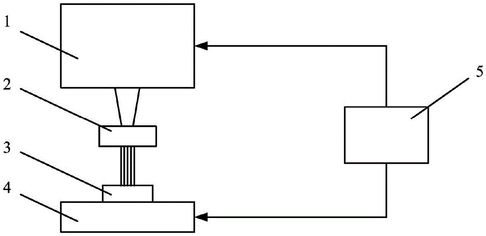
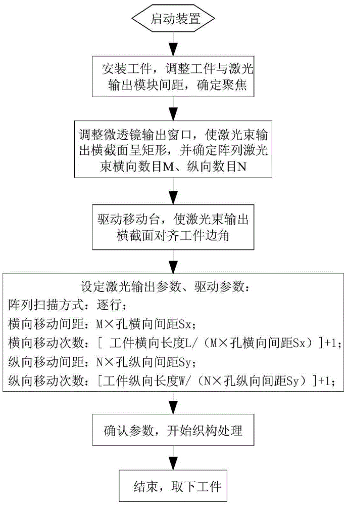
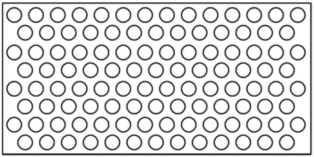
[0038] Such as figure 1 As shown, the microwave device surface texturing device of the present invention is composed of a laser output module 1 , a microlens 2 , a moving platform 4 and a control module 5 . The microwave device 3 to be processed is placed on the top surface of the mobile station 4, and the control module 5 outputs control signals to the laser output module 1 and the mobile station 4 to control the laser output power, the interval time, the moving distance and the moving time of the mobile station, and the microwave device is completed. 3 Surface deep hole array texture treatment. The laser beam can be a femtosecond laser or a nanolaser.

[0039] The working process of the microwave device surface texture device of the present invention is as follows: start the device, the control module 5 outputs a control signal to the laser output module 1, and the laser output module 1 is used to output a single beam of laser that can produce the effect of etching and remo...


PUM


Abstract

The invention provides a microwave device surface processing device capable of restraining secondary electron emission and a microwave device surface processing method capable of restraining secondary electron emission. The device consists of a laser output module, a micro lens, a movable table and a control module, wherein the control module outputs control signals to the laser output module and the movable table, so as to control the laser output power, the laser output interval time, the movement distance of the movable table and the movement time of the movable table; by virtue of a small-area deep hole array continuous moving and filling method, laser etching of a centimeter-scale large-area deep hole array structure on the surface of a microwave device is finished. The microwave device surface structure processed by the device and the method is of a rectangular uniformly-spaced or triangular uniformly-spaced micronano deep hole array, so that the secondary electron emission coefficient of the surface of the microwave device can be effectively reduced. The device and the method are automatic in processing, simple in process and high in efficiency, and can be used for performing processing treatment on the surfaces of parts such as gold or plated gold; the surface performance of the processed microwave device has long-term stability, and the processed microwave device is applicable to ground and aerospace environments.

Description

technical field [0001] The invention relates to a microwave device surface processing device and method, in particular to a microwave device surface processing device and a processing method capable of suppressing secondary electron emission. Background technique [0002] During the transmission of microwave signals by high-power microwave devices, the electrons in the microwave field will bombard the surface of the device under the action of microwave resonance, excite a large number of secondary electrons, and form a micro-discharge effect, which will seriously affect the microwave transmission performance and the device itself. damage. [0003] In order to improve the suppression performance of secondary electron emission on the surface of the device, the surface of the existing microwave device is mainly treated with nickel plating, gold plating, conductive oxidation and other surface treatments, and the secondary electron emission on the surface of the original material...

Claims


Application Information

Patent Timeline
Patent Type & Authority Patents(China)
IPC IPC(8): B23K26/352
CPCB23K26/352
Inventor 黄信林马小琴禹继芳苌群峰刘洪
Owner CHINA AEROSPACE TIMES ELECTRONICS CORP
Why Eureka
Try Eureka