
Method of forming a semiconductor device

A semiconductor and device technology, applied in the field of semiconductor device formation, can solve the problems of poor formation of fully surrounded gate nanowire transistors, etc., and achieve the effects of good electrical isolation performance, large selectivity, and easy removal

Active Publication Date: 2017-06-13
SEMICON MFG INT (SHANGHAI) CORP
View PDF5 Cites 0 Cited by
  • Summary
  • Abstract
  • Description
  • Claims
  • Application Information

AI Technical Summary

Problems solved by technology

[0006] However, the gate-all-around nanowire transistors formed by the prior art are poorly formed

Method used


Image

  • Method of forming a semiconductor device
  • Method of forming a semiconductor device
  • Method of forming a semiconductor device

Examples


Embodiment Construction

[0032] As mentioned in the background, the gate-all-around nanowire transistors formed by the prior art are poorly formed

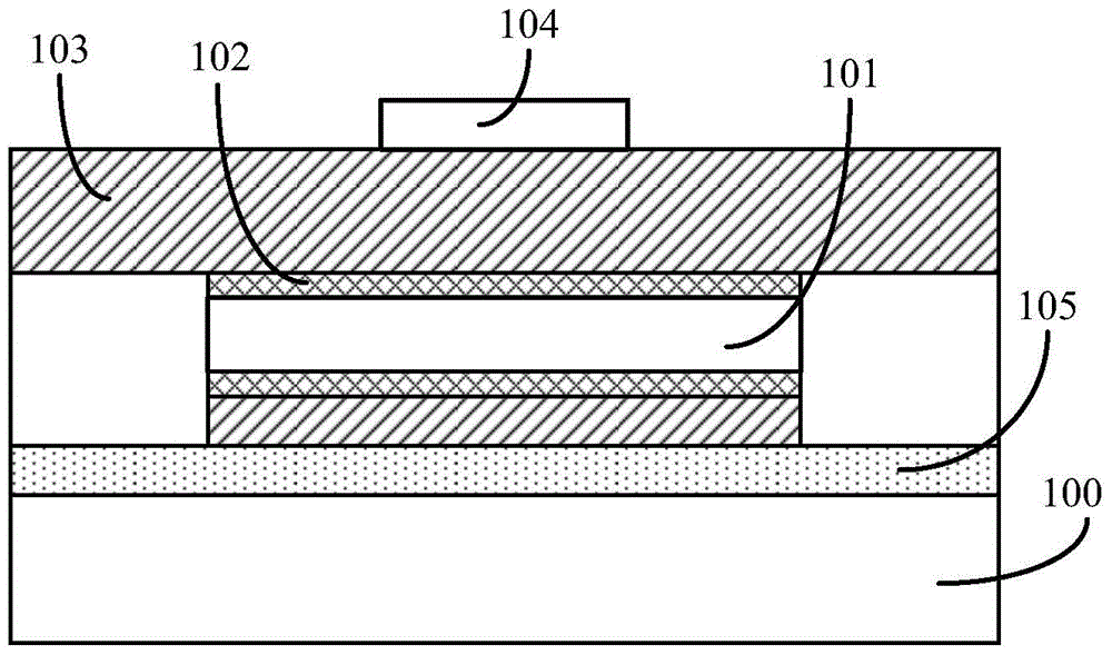
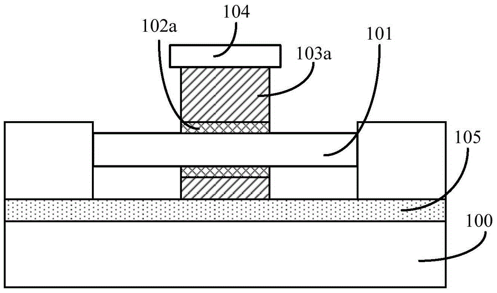
[0033] After research, it is found that after forming the nanowires suspended on the surface of the substrate, it is necessary to form a gate structure surrounding part of the nanowire surface, and the shape and size of the formed gate structure are poor, which easily leads to unstable performance of the formed transistor. . Specific as Figure 1 to Figure 2 As shown, is a schematic cross-sectional structure diagram of the process of forming the gate structure surrounding the nanowire.

[0034] Please refer to figure 1 A gate dielectric film 102 is formed on the surface of the nanowire 101 suspended from the surface of the substrate 100, a gate electrode film 103 is formed on the surface of the gate dielectric film 102, a mask layer 104 is formed on the surface of the gate electrode film 103, and the mask layer Layer 104 defines the corresponding locat...


PUM


Abstract

The invention discloses a forming method of a semiconductor device. The forming method comprises the following steps: providing a substrate, wherein discrete supporting parts and a nanowire suspended on the surface of a first dielectric layer are arranged on the surface of the substrate, and the two ends of the nanowire are respectively connected with the side walls of the adjacent supporting parts; forming a pseudo-grid membrane on the surface of the nanowire; adopting an anisotropic dry etching process to etch the pseudo-grid membrane and the nanowire until the first dielectric layer is exposed, enabling the pseudo-grid membrane to form a pseudo-grid electrode layer, and enabling the nanowire to form a nanowire channel structure encircled by the pseudo-grid electrode layer; adopting a selective deposition process to form a nanowire source / drain structure between the side wall of the nanowire channel structure and the side walls of the supporting parts; forming a second dielectric layer on the surfaces of the first dielectric layer, the pseudo-grid electrode layer and the nanowire source / drain structure, and enabling the surface of the second dielectric layer to be flush with the surface of the pseudo-grid electrode layer; then, removing the pseudo-grid electrode layer, and forming a gate structure in the opening. The formed semiconductor device is accurate in size and stable in performance.

Description

technical field [0001] The invention relates to the technical field of semiconductor manufacturing, in particular to a method for forming a semiconductor device. Background technique [0002] With the rapid development of semiconductor manufacturing technology, semiconductor devices are developing towards higher element density and higher integration. Transistors, as the most basic semiconductor devices, are currently being widely used. Therefore, as the component density and integration of semiconductor devices increase, the gate size of transistors is also getting shorter and shorter. However, the shortening of the gate size of the transistor will cause the short-channel effect of the transistor, thereby generating leakage current, and ultimately affecting the electrical performance of the semiconductor device. [0003] In order to overcome the short channel effect of the transistor and suppress the leakage current, the prior art proposes a fully surrounded gate nanowire ...

Claims


Application Information

Patent Timeline
Patent Type & Authority Patents(China)
IPC IPC(8): H01L21/28
CPCH01L29/413H01L29/42308H01L29/43H01L29/66545
Inventor 洪中山
Owner SEMICON MFG INT (SHANGHAI) CORP
Learn More