Method of forming semiconductor device

A semiconductor and device technology, which is applied in the field of semiconductor device formation, can solve the problems such as the electrical performance of semiconductor devices needs to be improved, and achieve the effect of improving the short channel effect, improving corrosion resistance, and reducing the probability of diffusion to the channel region

Active Publication Date: 2017-11-03
SEMICON MFG INT (SHANGHAI) CORP
View PDF3 Cites 0 Cited by
  • Summary
  • Abstract
  • Description
  • Claims
  • Application Information

AI Technical Summary

Problems solved by technology

[0005] However, in the formation process of the actual semiconductor device, it is found that despite the LDD process, the short channel effect in the semiconductor device still exists, and the electrical performance of the semiconductor device still needs to be improved

Method used


Image

  • Method of forming semiconductor device
  • Method of forming semiconductor device
  • Method of forming semiconductor device

Examples


Embodiment Construction

[0035] It can be known from the background art that there is a short channel effect in semiconductor devices formed in the prior art.

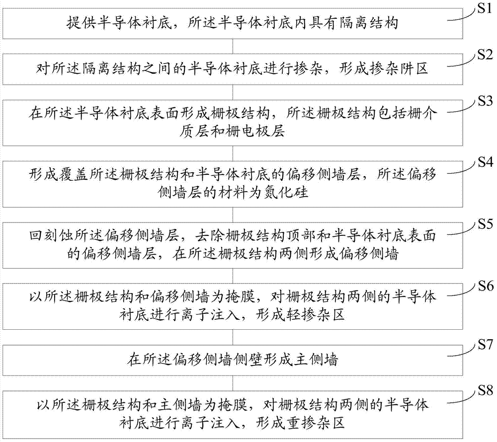
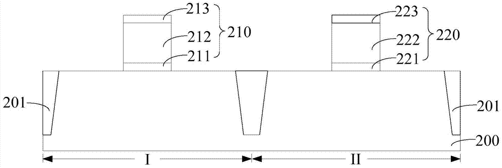
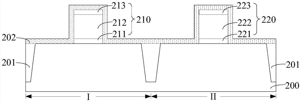
[0036] In order to solve the above-mentioned problems, research is conducted on the formation method of semiconductor devices. The formation method of semiconductor devices includes the following steps, please refer to figure 1 : Step S1, providing a semiconductor substrate with isolation structures in the semiconductor substrate; step S2, doping the semiconductor substrate between the isolation structures to form doped well regions; step S3; in the semiconductor substrate A gate structure is formed on the surface of the substrate, the gate structure includes a gate dielectric layer and a gate electrode layer; step S4, an offset spacer layer covering the gate structure and the semiconductor substrate is formed, the offset spacer layer The material is silicon nitride; step S5, etch back the offset sidewall layer, remove the offset sidewall layer on...


PUM


Abstract

A method for forming a semiconductor device comprises the following steps: providing a semiconductor substrate, wherein gate structures are formed on the surface of the semiconductor substrate; forming offset spacers at the two sides of the gate structures; performing co-doping (including first doping and second doping) on the offset spacers, wherein the first doping is used for capturing defects in the offset spacers, and the second doping improves the content of doped ions in the regions, near the surface of the semiconductor substrate, of the offset spacers; forming lightly doped regions in the semiconductor substrate at the two sides of the gate structures by using the offset spacers as masks; forming main spacers on the side walls of the offset spacers; and forming heavily doped regions in the semiconductor substrate at the two sides of the gate structures by using the main spacers as masks. According to a semiconductor device formed by the method of the invention, the content of boron ions in the semiconductor substrate below the offset spacers is reduced, the probability that boron ions diffuse into a channel region is reduced, the short channel effect of the semiconductor device is improved, and the electrical performance of the semiconductor device is optimized.

Description

Technical field [0001] The present invention relates to the field of semiconductor manufacturing technology, and in particular to a method for forming semiconductor devices. Background technique [0002] The main semiconductor devices of integrated circuits, especially VLSIs, are metal-oxide-semiconductor field effect transistors (MOS transistors). With the continuous development of integrated circuit manufacturing technology, the technology nodes of semiconductor devices continue to decrease, and the geometric dimensions of semiconductor devices continue to shrink in accordance with Moore's Law. [0003] With the rapid development of semiconductor manufacturing technology, the feature size (CD) of semiconductor devices has entered the sub-micron stage. In order to obtain faster operation speed, greater data storage capacity and more functions, semiconductor integrated circuits are constantly developing in the direction of higher component density and high integration. As the bas...

Claims


Application Information

Patent Timeline
Patent Type & Authority Patents(China)
IPC IPC(8): H01L21/8238H01L21/336
CPCH01L21/8238H01L21/823864H01L27/092
Inventor 何有丰
Owner SEMICON MFG INT (SHANGHAI) CORP
Why Eureka
Try Eureka