Dual-waveband photoelectric detector and preparation method thereof
A photodetector and dual-band technology, applied in the direction of circuits, electrical components, semiconductor devices, etc., can solve the problems of complex materials and preparation processes, and the inability to realize simultaneous and same-position detection, so as to achieve detection, cost saving, and sensitive detection Effect
- Summary
- Abstract
- Description
- Claims
- Application Information
AI Technical Summary
Problems solved by technology
Method used
Image

Examples
Embodiment Construction
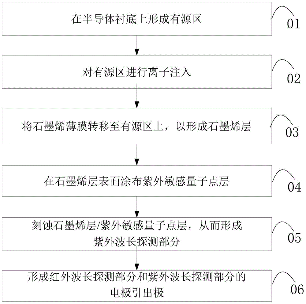
[0032] In order to make the content of the present invention clearer and easier to understand, the content of the present invention will be further described below in conjunction with the accompanying drawings. Of course, the present invention is not limited to this specific embodiment, and general replacements known to those skilled in the art are also covered within the protection scope of the present invention.
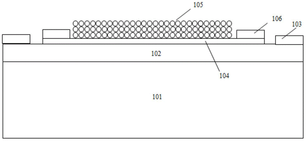
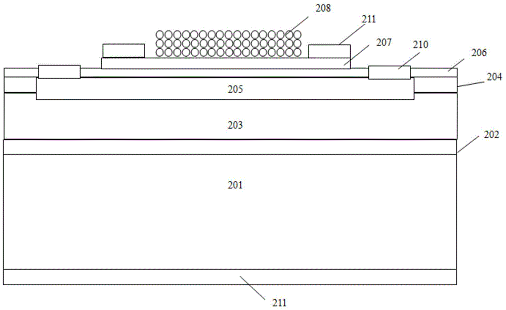
[0033] The dual-band photodetector of the present invention includes: a semiconductor substrate; an infrared wavelength detection part with an ion-implanted active region on the semiconductor substrate; an ultraviolet wavelength detection part on the infrared wavelength detection part, and an infrared wavelength detection part. The wavelength detection part and the electrode extraction pole of the ultraviolet wavelength detection part; wherein, the ultraviolet wavelength detection part includes; a graphene layer located on the active area of the infrared wavelengt...
PUM
 Abstract
Description
Claims
Application Information
 - R&D
- Intellectual Property
- Life Sciences
- Materials
- Tech Scout
- Unparalleled Data Quality
- Higher Quality Content
- 60% Fewer Hallucinations
Browse by: Latest US Patents, China's latest patents, Technical Efficacy Thesaurus, Application Domain, Technology Topic, Popular Technical Reports.
© 2025 PatSnap. All rights reserved.Legal|Privacy policy|Modern Slavery Act Transparency Statement|Sitemap|About US| Contact US: help@patsnap.com