Photovoltaic materials and their preparation methods and applications

A photovoltaic material and atomic technology, applied in the field of solar cells, can solve problems such as increasing efficiency, high cost, and reducing cost

Active Publication Date: 2016-08-24
SHENZHEN INST OF ADVANCED TECH +1
View PDF4 Cites 0 Cited by
  • Summary
  • Abstract
  • Description
  • Claims
  • Application Information

AI Technical Summary

Problems solved by technology

However, the cost of indium and gallium is relatively high, so it is of great significance to modify the intermediate band of broadband copper-based materials to reduce costs and increase efficiency.

Method used


Image

  • Photovoltaic materials and their preparation methods and applications
  • Photovoltaic materials and their preparation methods and applications
  • Photovoltaic materials and their preparation methods and applications

Examples


preparation example Construction

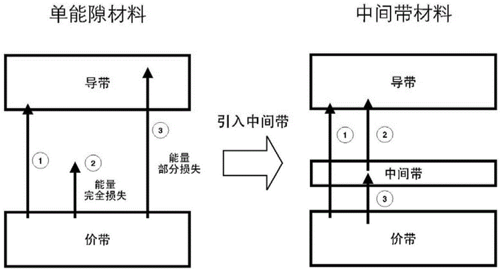
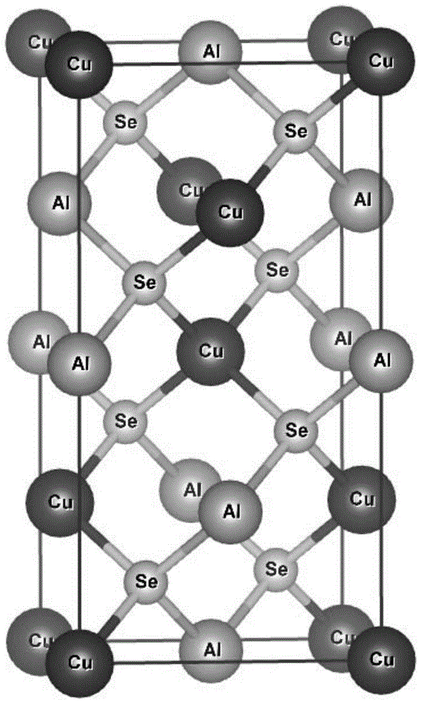
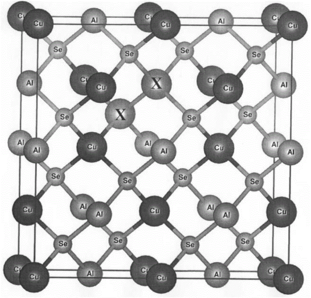
[0024] In the preparation process of the above-mentioned photovoltaic material, different chemical ratios are used, which will produce different impurity phases in the semiconductor material. Specific impurity phases can be produced by precise stoichiometry. In order to manufacture special functional materials. According to calculations, when Al and Se have an accurate ratio of 1:2, the doped P will replace Al and Se atoms at the same time, and the substitution of P for Al and Se will produce ions with different electrical properties. The positions of Al and Se tend to be close to each other to form stable substitution pairs, which will help the formation of high-concentration doped materials. This substitution has the effect of forming a new intermediate band in the original energy gap. The density of states in the middle band is determined by the doping concentration of P. In particular, a more reasonable doping concentration is between 5% and 20%.

[0025] Figure 4-6 ...

Embodiment 1

[0045] see Figure 8 , Figure 8 It is a schematic diagram of the structure of the vapor deposition sample equipment. Figure 7 11, 12, 13 and 14 are heating source furnaces for Cu, Al, Se and doping element X respectively. The shutter 20 is used to close the source port in time when the evaporation ends. Molecular beams formed when Cu, Al, Se and dopant elements are heated and evaporated. The substrate 30 is provided between the heater 40 and the heat source furnaces 11 , 12 , 13 , and 14 .

[0046] First, put the prepared soda-lime glass coated with 1 μm thick Mo as the substrate on the sample holder, close the sampling window, and use the co-evaporation method to simultaneously heat the source furnace of Cu, Al, P, and Se in the MBE chamber The target material in the present invention obtains a photovoltaic material with an atomic ratio of Cu:Al:P:Se=1.0:0.9:0.2:1.9. Among them, the temperature of the substrate is 400°C, and the temperatures of the source furnaces of C...

Embodiment 2

[0048] Put the prepared soda-lime glass coated with Mo with a thickness of 1 μm as the substrate on the sample holder, close the sampling window, and use the co-evaporation method to simultaneously heat the source furnaces of Cu, Al, As, and Se in the MBE chamber, A photovoltaic material with an atomic ratio of Cu:Al:As:Se=1.0:0.95:0.1:1.95 is obtained. Among them, the temperature of the substrate is 420°C, and the temperatures of the source furnaces of Cu, Al, As, and Se are 1260°C, 710°C, 800°C, and 280°C, respectively.


PUM

PropertyMeasurementUnit
thicknessaaaaaaaaaa

Abstract

The invention discloses a photovoltaic material. The molecular formula of the photovoltaic material is CuAl(1-y)Se(2-y)X2y, the photovoltaic material adopts an orthorhombic chalcopyrite-type structure similar to CuAlSe2, X substitutes the lattice positions of partial Al atoms and Se atoms, y is equal to 0.05-0.2, and X is a V-group element. The material can absorb both near-infrared sunlight and visible-band sunlight. When the novel material is taken as an absorbed layer to manufacture a photovoltaic device, the material has the high voltage characteristic of a wide band gap semiconductor and also has the high current characteristic of a narrow band gap material, so that the photovoltaic device has higher conversion efficiency. Moreover, the photovoltaic material does not contain indium and gallium, so that the cost is reduced.

Description

technical field [0001] The invention relates to the field of solar cells, in particular to a photovoltaic material, a preparation method thereof and an application in solar cells. Background technique [0002] In recent years, the development of solar cell materials has gradually shifted from the first-generation solar cells represented by crystalline silicon to the second-generation thin-film solar cells with lower costs. The development of the first-generation solar cells represented by crystalline silicon and the second-generation thin-film solar cells has become increasingly mature. However, both types of cells use a single energy gap to absorb solar energy, and photons with energy lower than the energy gap cannot be utilized ( figure 1 Left 2 process), while the energy of photons with energy higher than the energy gap cannot be completely converted ( figure 1 Left 3 process), so according to the Shockley-Queisser theory, the limit conversion efficiency can only reach ...

Claims


Application Information

Patent Timeline
Patent Type & Authority Patents(China)
IPC IPC(8): C01B19/00H01L31/032
Inventor 薛艳君李晓光顾光一钟国华武光芬李朝辉罗海林杨春雷肖旭东
Owner SHENZHEN INST OF ADVANCED TECH
Why Eureka
Try Eureka