Supercharge Your Innovation With Domain-Expert AI Agents!

Organic electroluminescence device and preparing method thereof

An electroluminescent device and electroluminescent technology, which are applied in the fields of electric solid state devices, semiconductor/solid state device manufacturing, electrical components, etc., can solve the problems of low exciton recombination probability and low luminous efficiency, etc.

Inactive Publication Date: 2015-06-24
OCEANS KING LIGHTING SCI&TECH CO LTD +2
View PDF0 Cites 2 Cited by
  • Summary
  • Abstract
  • Description
  • Claims
  • Application Information

AI Technical Summary

Problems solved by technology

[0003] In the field of traditional organic electroluminescence, the electron transport rate is two or three orders of magnitude lower than the hole transport rate, so it is very easy to cause the low probability of exciton recombination, and the area where the recombination is not in the light-emitting area, resulting in luminescence Reduced efficiency

Method used


Image

  • Organic electroluminescence device and preparing method thereof
  • Organic electroluminescence device and preparing method thereof
  • Organic electroluminescence device and preparing method thereof

Examples


preparation example Construction

[0044] Such as figure 2 The preparation method of the above-mentioned organic electroluminescence device shown, comprises the following steps:

[0045] S10 , performing surface pretreatment on the substrate 10 .

[0046] The substrate 10 is glass. Generally speaking, ordinary glass will do. In special application fields, special glass made by special process can also be selected.

[0047] The surface pretreatment process specifically includes: after the substrate 10 is rinsed with distilled water and ethanol in sequence, it is soaked in isopropanol overnight.

[0048] S20 , preparing the anode 20 on the substrate 10 by magnetron sputtering.

[0049] The anode 20 may be an indium tin oxide film (ITO), an aluminum-doped zinc oxide film (AZO) or an indium-doped zinc oxide film (IZO), and the thickness of the anode 20 is 50 nm to 300 nm. In a preferred embodiment, the anode 20 is an indium tin oxide film (ITO), and the thickness of the anode 20 is 120 nm.

[0050] The accel...

Embodiment 1

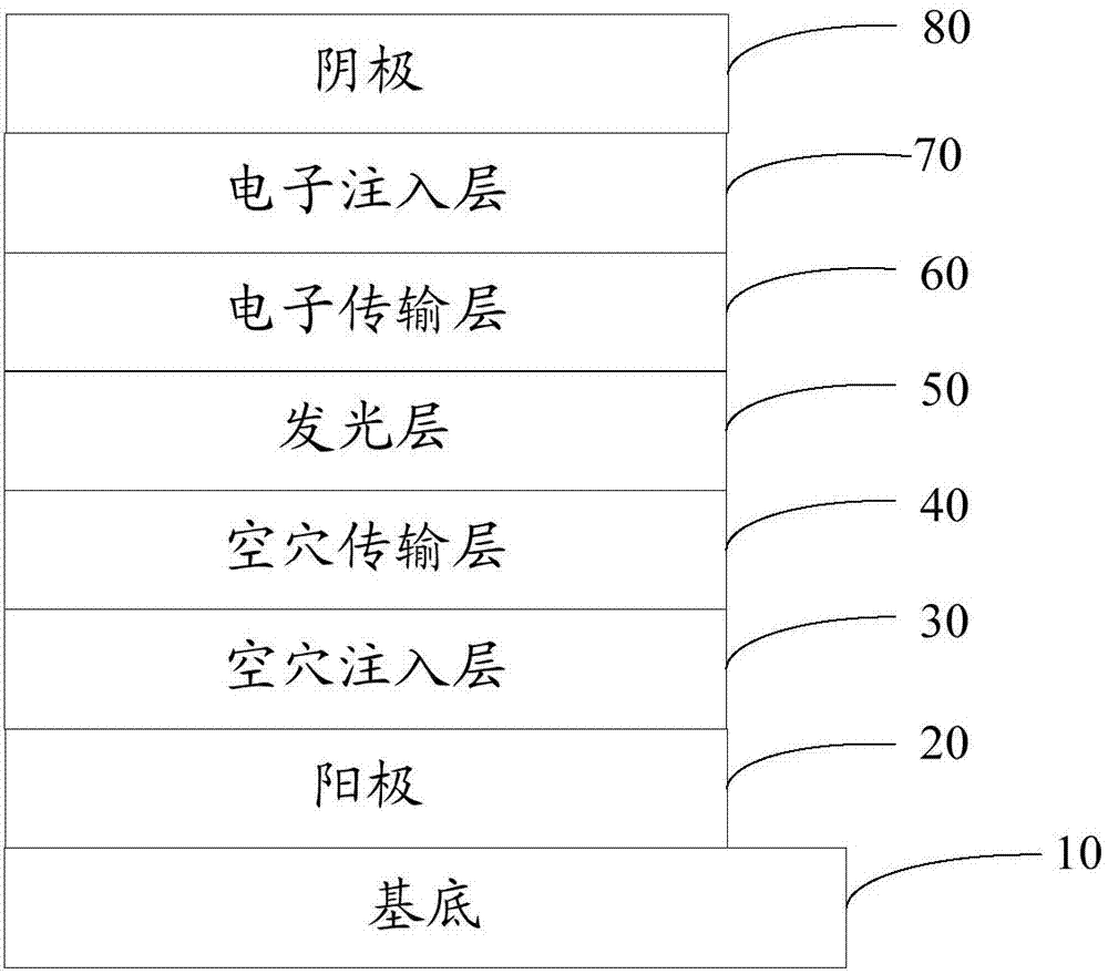
[0067] An organic electroluminescent device, including a substrate, an anode, a hole injection layer, a hole transport layer, a light emitting layer, an electron transport layer, an electron injection layer and a cathode stacked in sequence, the specific structure is expressed as: glass / ITO / MoO 3 / NPB / BCzVBi / TPBI / BCP:3HT:F4-TCNQ / Ag. The preparation steps are:

[0068] Provide a commercially available common glass, rinse the glass with distilled water and ethanol in sequence, and soak it in isopropanol overnight.

[0069] The anode was prepared by magnetron sputtering on the surface-treated glass surface. The material of the anode is ITO, and the thickness is 120nm. The acceleration voltage of magnetron sputtering is 700V, the magnetic field is 120G, and the power density is 25W / cm 2 .

[0070] The working pressure is 8×10 -4 Under the condition of Pa, the evaporation rate of organic materials is 0.2nm / s, and the evaporation rate of metals and metal compounds is 2nm / s, and...

Embodiment 2

[0076] An organic electroluminescent device, including a substrate, an anode, a hole injection layer, a hole transport layer, a light emitting layer, an electron transport layer, an electron injection layer and a cathode stacked in sequence, the specific structure is expressed as: glass / IZO / V 2 o 5 / TAPC / AND / TAZ / Bphen:3AT:1T-NATA / Al. The preparation steps are:

[0077] Provide a commercially available common glass, rinse the glass with distilled water and ethanol in sequence, and soak it in isopropanol overnight.

[0078] The anode was prepared by magnetron sputtering on the surface-treated glass surface. The material of the anode is IZO with a thickness of 300nm. The acceleration voltage of magnetron sputtering is 300V, the magnetic field is 50G, and the power density is 40W / cm 2 .

[0079] The working pressure is 2×10 -3 Under the condition of Pa, according to the vapor deposition rate of the organic material is 1nm / s, and the vapor deposition rate of the metal and met...


PUM


Abstract

The invention discloses an organic electroluminescence device. The device comprises a substrate, an anode, a hole injection layer, a hole transmission layer, a light emitting layer, an electron transmission layer, an electron injection layer and a cathode which are overlapped in sequence. The electron injection layer of the organic electroluminescence device is made of mixtures of electron transmission materials, thiophene compounds and hole doping object materials. The electron transmission materials can be subjected to crystallization easily under the vitrification converting temperature of 50-100 DEG C, electron transmission speed can be improved, crystallization can happen easily, after crystallization, crystal arraying is in order, light scattering can be enhanced, light emitted to the two sides is scattered back to the middle to be emitted out, and light-out efficiency is improved. Compared with a traditional organic electroluminescence device, the organic electroluminescence device is high in light-emitting efficiency. The invention further discloses a preparing method of the organic electroluminescence device.

Description

technical field [0001] The invention relates to the field of organic electroluminescence, in particular to an organic electroluminescence device and a preparation method thereof. Background technique [0002] In 1987, C.W.Tang and Van Slyke of Eastman Kodak Company in the United States reported a breakthrough in the research of organic electroluminescence. A high-brightness, high-efficiency double-layer organic electroluminescent device (OLED) has been prepared using ultra-thin film technology. The brightness reaches 1000cd / m2 at 10V, the luminous efficiency is 1.51lm / W, and the lifespan is more than 100 hours. [0003] In the field of traditional organic electroluminescence, the electron transport rate is two or three orders of magnitude lower than the hole transport rate, so it is very easy to cause the low probability of exciton recombination, and the area where the recombination is not in the light-emitting area, resulting in luminescence Reduced efficiency. Contents...

Claims


Application Information

Patent Timeline
Patent Type & Authority Applications(China)
IPC IPC(8): H01L51/52H01L51/54H01L51/56
CPCH10K85/00H10K85/649H10K85/6565H10K85/6572H10K50/171H10K71/00
Inventor 周明杰黄辉陈吉星王平
Owner OCEANS KING LIGHTING SCI&TECH CO LTD
Features
  • R&D
  • Intellectual Property
  • Life Sciences
  • Materials
  • Tech Scout
  • Unparalleled Data Quality
  • Higher Quality Content
  • 60% Fewer Hallucinations
Learn More