Preparation method for motion sensor

A motion sensor and device technology, applied in the manufacture of microstructure devices, techniques for producing decorative surface effects, decorative art, etc., can solve problems such as filling metals are easy to form holes, temperature rises, and device operating voltages increase

Active Publication Date: 2015-07-01
SEMICON MFG INT (SHANGHAI) CORP
View PDF8 Cites 4 Cited by
  • Summary
  • Abstract
  • Description
  • Claims
  • Application Information

AI Technical Summary

Problems solved by technology

[0005] Further, in order to form an electrical connection with the MEMS substrate 103 and the base 101, etch the MEMS substrate 103, the dielectric layer to the conductive layer, the etching method is the DRIE method, but due to the vias formed in the DRIE method The hole has a high aspect ratio, generally (aspect ratio) is 10-15:1 or even higher, and the opening size of the through hole is generally less than 5um, filling the trench with a large aspect ratio with metal When it is easy to enclose the air and form holes, the resistance of the through hole will increa

Method used


Image

  • Preparation method for motion sensor
  • Preparation method for motion sensor
  • Preparation method for motion sensor

Examples


Embodiment 1

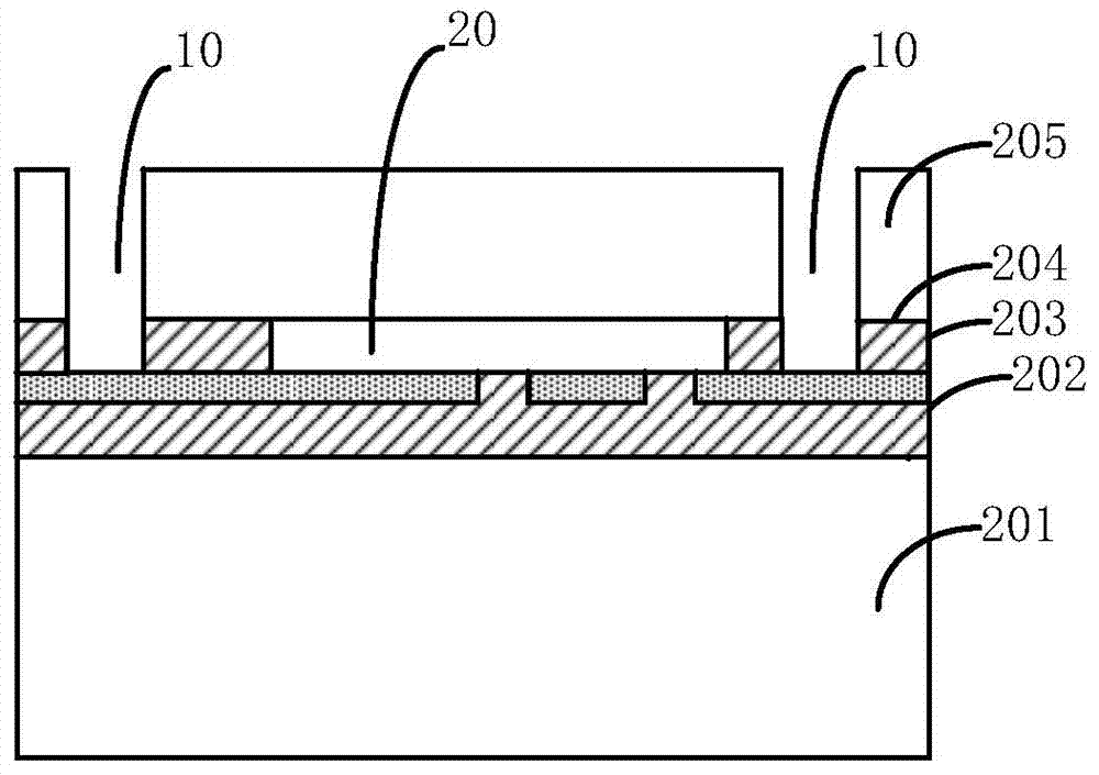
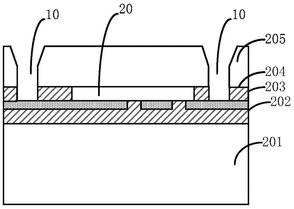
[0059] Attached below Figure 2a-2f A specific embodiment of the present invention will be further described.

[0060] Firstly, step 201 is performed to provide a substrate 201 on which CMOS devices are formed.

[0061] Specifically, refer to Figure 2a , the base 201 includes a semiconductor substrate, and various active devices formed on the substrate, wherein the semiconductor substrate can be at least one of the materials mentioned below: silicon, silicon-on-insulator (SOI), silicon-on-insulator (SSOI), silicon-germanium-on-insulator (S-SiGeOI), silicon-germanium-on-insulator (SiGeOI) and germanium-on-insulator (GeOI), etc.

[0062] Various active devices are formed on the semiconductor substrate, for example, CMOS devices and other active devices are formed on the semiconductor substrate, and the active devices are not limited to a certain type.

[0063] Next, step 202 is performed to form a bottom electrode 203 on the substrate 201 .

[0064] Specifically, the method...


PUM


Abstract

The invention relates to a preparation method for a motion sensor. The method includes: providing a base, on which a CMOS device is formed; forming a bottom electrode on the base and an MEMS substrate positioned above the bottom electrode, and forming a cavity between the bottom electrode and the MEMS substrate; etching the MEMS substrate to the bottom electrode to form a deep through hole, thereby exposing the bottom electrode; etching the top of the deep through hole to expand the key size of the deep through hole top opening; forming an insulation layer on the side wall of the deep through hole; and depositing a metal material in the deep through hole, and then conducting etching to remove the metal material deposited at the deep through hole top so as to maintain a large key size of the opening. According to the method provided by the invention, no hole is formed in the filling process, and the device yield is improved.

Description

technical field [0001] The invention relates to the field of semiconductors, and in particular, the invention relates to a method for preparing a motion sensor. Background technique [0002] With the continuous development of semiconductor technology, smartphones, integrated CMOS and micro-electromechanical systems (MEMS) devices have increasingly become the most mainstream and advanced technologies in the market for motion sensor products, and with technology updates , the development direction of this type of transmission sensor products is smaller size, high-quality electrical performance and lower loss. [0003] In the prior art, a deep reactive ion etching (DRIE) system is required most of the time to prepare the motion sensor, and reactive ion etching is one of the important processes in integrated circuit manufacturing, MEMS processing and other device processing . It is mainly used for the etching of various thin films such as polysilicon, silicon nitride, silicon ...

Claims


Application Information

Patent Timeline
IPC IPC(8): B81C1/00
Inventor 谢红梅许继辉于佳
Owner SEMICON MFG INT (SHANGHAI) CORP
Why Eureka
Try Eureka