

Semiconductor device forming method
A semiconductor and device technology, applied in the field of semiconductor device formation, can solve the problems of silicon loss, reduce the signal transmission rate of the core circuit, etc., and achieve the effect of high carrier mobility and high signal transmission rate
- Summary
- Abstract
- Description
- Claims
- Application Information
AI Technical Summary
Problems solved by technology
Method used
Image

Examples
Embodiment Construction
[0047] In order to make the above objects, features and advantages of the present invention more comprehensible, specific embodiments of the present invention will be described in detail below in conjunction with the accompanying drawings.
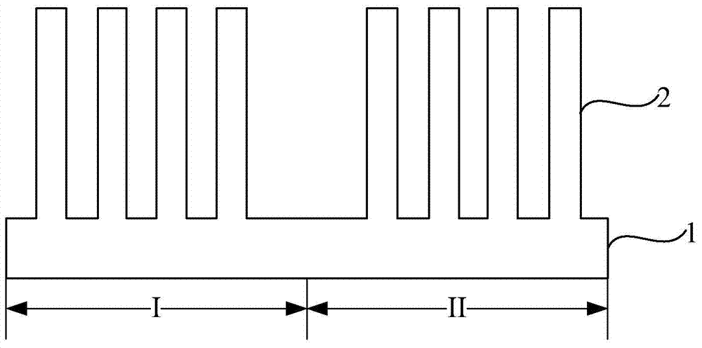
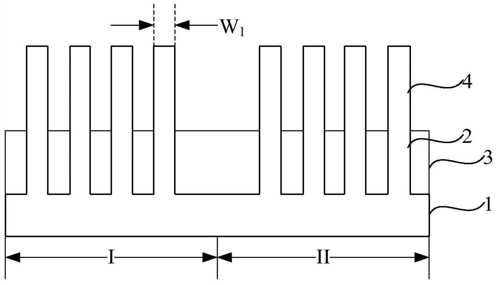
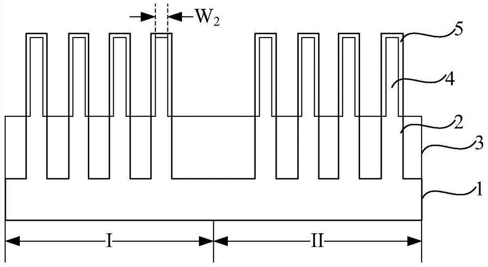
[0048] refer to Figure 4 , providing a substrate 100, the substrate 100 includes a core area I and a peripheral area II, the core area I will be used to form a core circuit, and the peripheral area II will be used to form an I / O circuit.
[0049] In a specific embodiment, the substrate 100 may be a silicon substrate, or may be a germanium, silicon germanium, gallium arsenide or silicon-on-insulator substrate. Those skilled in the art can select the substrate according to needs, so the type of the substrate should not limit the protection scope of the present invention. A silicon substrate is selected as the substrate 100 in this embodiment, because the cost of implementing the technical solution on a silicon substrate is lower than that ...
PUM
 Abstract
Description
Claims
Application Information