ITO film and preparation method thereof as well as LED chip and preparation method thereof

A technology of LED chips and thin films, applied in electrical components, circuits, semiconductor devices, etc., can solve the problems of increased process time, low process efficiency, poor process quality, etc., to improve process quality, improve process efficiency, and reduce driving voltage. Effect

Inactive Publication Date: 2015-07-01
BEIJING NAURA MICROELECTRONICS EQUIP CO LTD
View PDF3 Cites 6 Cited by
  • Summary
  • Abstract
  • Description
  • Claims
  • Application Information

AI Technical Summary

Problems solved by technology

[0006] First, since the annealing process is added after the deposition of the ITO interface layer, the process flow is increased, resulting in an increase in the required process time and low process efficiency; and because the annealing process needs to be in contact with the atmospheric environment with more impurities, it is possible It affects the ITO current spreading layer, resulting in poor process quality;
[0007] Second, although the ITO interface layer can reduce the interface resistance between the ITO film and the P-GaN layer, the ITO interface layer and the ITO current diffusion layer with different compositions will introduce new interface resistance, which is not conducive to reducing the driving voltage of the LED chip.

Method used


Image

  • ITO film and preparation method thereof as well as LED chip and preparation method thereof
  • ITO film and preparation method thereof as well as LED chip and preparation method thereof
  • ITO film and preparation method thereof as well as LED chip and preparation method thereof

Examples


preparation example Construction

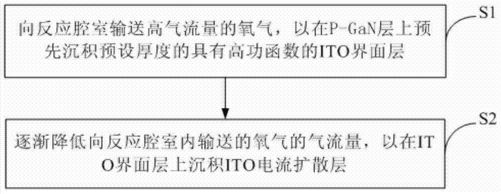
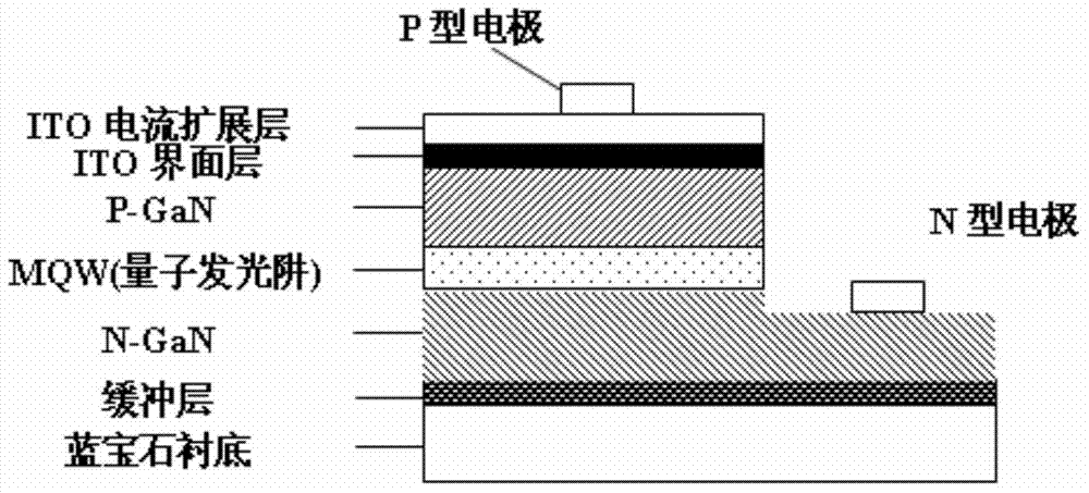
[0031] figure 1 The flow chart of the preparation method of the ITO thin film provided by the embodiment of the present invention. figure 2 It is a schematic structural diagram of an LED chip with an ITO thin film prepared by the preparation method of the ITO thin film provided in this embodiment. Please also refer to figure 1 with figure 2, ITO thin film comprises ITO interface layer and ITO current diffusion layer, the preparation method of the ITO thin film that the present embodiment provides at least comprises the following steps:

[0032] Step S1, delivering high gas flow oxygen into the reaction chamber to pre-deposit an ITO interface layer with a high work function of a preset thickness on the P-GaN layer;

[0033] Step S2, gradually reducing the flow rate of the oxygen gas supplied to the reaction chamber, so as to deposit an ITO current diffusion layer with a graded structure on the ITO interface layer.

[0034] In this embodiment, the ITO interface layer is de...


PUM


Abstract

The invention provides an ITO film and a preparation method thereof as well as an LED chip and a preparation method thereof. The preparation method of the ITO film at least comprises the steps that 1) oxygen of high flow is transmitted into a reaction chamber, so that an ITO interfacial layer of high work function and a preset thickness is pre-deposited on a P-GaN layer; and 2) the flow of the oxygen transmitted to the reaction chamber is gradually reduced, so that an ITO current diffusion layer is deposited on the ITO interfacial layer. The preparation method of the ITO film can be used to reduce the driving voltage of the LED chip, and improve the technical efficiency and quality.

Description

technical field [0001] The invention belongs to the technical field of semiconductor processing, and in particular relates to an ITO thin film and a preparation method thereof, an LED chip and a preparation method thereof. Background technique [0002] In the process of LED chip manufacturing, because the contact between P-GaN layer and P-type ohmic metal electrode will cause high contact resistance and low transmittance, the driving voltage of LED chip will increase, and the higher driving voltage will make LED During the use of the chip, a large amount of heat is generated, which not only causes energy loss, but also affects the reliability of the LED chip, thereby affecting the overall performance of the LED chip. [0003] In practical applications, compared with traditional metal films, ITO films have the advantages of high transmittance, good electrical conductivity, wear resistance, corrosion resistance, etc., and have good adhesion to GaN layers. Therefore, ITO films ...

Claims


Application Information

Patent Timeline
Patent Type & Authority Applications(China)
IPC IPC(8): H01L33/00H01L33/42
CPCH01L33/005H01L33/42H01L2933/0016
Inventor 王宽冒耿波荣延栋王厚工丁培军
Owner BEIJING NAURA MICROELECTRONICS EQUIP CO LTD
Why Eureka
Try Eureka