

Wafer bonding detection structure, preparation method and detection method
A detection structure, wafer bonding technology, applied in the direction of microstructure technology, microstructure devices, manufacturing microstructure devices, etc., can solve the problems of unusable devices, inability to fully reflect the bonding quality of the entire wafer, destructive testing, etc. , to achieve the effect of covering a wide area
- Summary
- Abstract
- Description
- Claims
- Application Information
AI Technical Summary
Problems solved by technology
Method used
Image

Examples
Embodiment 1
[0062] Figure 2e It is a structural schematic diagram of the test structure in a specific embodiment of the present invention, wherein Figure 2e The figure on the right is a partial enlarged view of the marked area in the figure on the left;
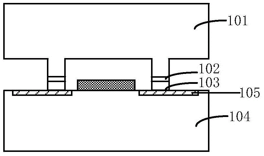
[0063] The test structure includes a bond between two wafers, wherein the lower one is a wafer forming MEMS components, and the wafer includes a semiconductor substrate (not shown in the figure), and the semiconductor Various materials commonly used in this field can be selected, and various devices, such as various CMOS devices, etc., are also formed in the semiconductor substrate, so that the CMOS process and the MEMS process will be combined to form a CMEMS process, and the formed Both the device and the forming method can be designed and manufactured as required, and will not be repeated here.
[0064] The test structure also includes a MEMS substrate 204 on which MEMS components are formed, wherein the type of the MEMS component...
Embodiment 2
[0081] The present invention also provides a method for selecting the above-mentioned test structure to detect the quality of wafer bonding. In the method, the resistance test device is connected to the interconnection metal layer 205 through the probe of WAT, and the voltage is applied The resistance value is measured in the case where the current flows as image 3 As shown, the current enters the joint interface in the figure through the interconnected metal layer at one end of the MEMS substrate 204, and then enters the conductive material layer 203 through the joint interface, and after flowing through the conductive material layer 203 Enter the bonding interface at the other end, finally to the interconnection metal layer at the other end in the MEMS substrate 204, then connect to the resistance testing device through the probe of WAT, the resistance tested in this process is the interconnection metal layer 205 , the bonding interface and the conductive material layer 203...
Embodiment 3
[0089] In the present invention, the test structure is realized by changing the manufacturing process flow of the MEMS device without affecting the device structure, so the test structure changes the destructive test in the prior art.
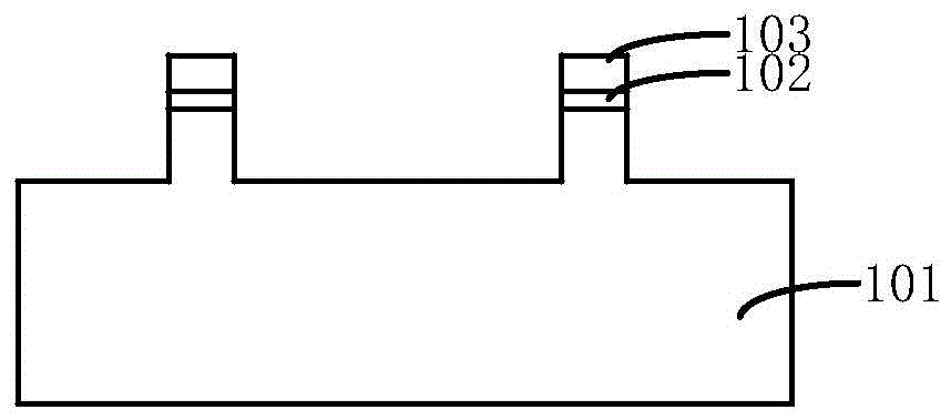
[0090] Attached below Figure 2a-2e The preparation method of the test structure described in the present invention is further described.
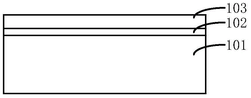
[0091] Firstly, step 201 is executed, a semiconductor substrate 201 is provided, and an isolation layer 202 is formed on the semiconductor substrate 201 .
[0092] Specifically, refer to Figure 2a , the semiconductor substrate 201 can be selected from commonly used semiconductor materials in the field, and in this embodiment, the semiconductor substrate 201 is selected from silicon.
[0093] Wherein, the isolation layer 202 can be selected from commonly used insulating materials in the field, such as SiO 2 , SiN, carbon-doped silicon oxide (SiOC), or silicon carbonitride (SiCN), etc. Alternatively, a t...
PUM
 Abstract
Description
Claims
Application Information