Graphene/indium phosphide photoelectric detector and preparation method thereof
A photodetector, indium phosphide technology, which is applied to circuits, electrical components, semiconductor devices, etc., can solve problems such as affecting the responsivity of light detection, achieve good light absorption and light detection response performance, is easy to implement, and has a simple preparation process Effect
- Summary
- Abstract
- Description
- Claims
- Application Information
AI Technical Summary
Problems solved by technology
Method used
Image

Examples
Embodiment 1
[0023] 1) Immerse the p-type indium phosphide sheet sample successively in acetone and isopropanol solutions for surface cleaning;
[0024] 2) Transfer the single-layer graphene to the cleaned indium phosphide sheet;
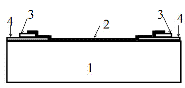
[0025] 3) A 100nm gold electrode is deposited on the graphene by a thermal evaporation process to obtain a graphene / indium phosphide photodetector.
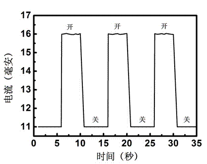
[0026] Apply a voltage between the two surface electrodes, and test the photodetector's current change under different light conditions to reflect its response to different spectra and light intensities. image 3 That is, when 5V voltage is applied to the photodetector prepared in this example, the current value change curves of continuous tests at intervals without illumination and under 1 standard sunlight illumination can be seen that the photodetector prepared in this example has a sensitive photoresponse, High responsiveness.
Embodiment 2
[0028] 1) Immerse the n-type indium phosphide sheet in acetone and isopropanol solutions successively for surface cleaning;
[0029] 2) Transfer 10 layers of graphene to the cleaned indium phosphide sheet;
[0030] 3) Deposit 200nm nickel / gold electrodes on graphene by thermal evaporation process to obtain graphene / indium phosphide photodetectors.
Embodiment 3
[0032] 1) Immerse the n-type indium phosphide sheet in acetone and isopropanol solutions successively for surface cleaning;
[0033] 2) Transfer the 3-layer graphene onto the cleaned indium phosphide sheet;
[0034] 3) Screen-print 500nm silver electrodes on graphene to obtain graphene / indium phosphide photodetectors.
PUM
| Property | Measurement | Unit |
|---|---|---|
| Thickness | aaaaa | aaaaa |
Abstract
Description
Claims
Application Information
 - R&D
- Intellectual Property
- Life Sciences
- Materials
- Tech Scout
- Unparalleled Data Quality
- Higher Quality Content
- 60% Fewer Hallucinations
Browse by: Latest US Patents, China's latest patents, Technical Efficacy Thesaurus, Application Domain, Technology Topic, Popular Technical Reports.
© 2025 PatSnap. All rights reserved.Legal|Privacy policy|Modern Slavery Act Transparency Statement|Sitemap|About US| Contact US: help@patsnap.com