Manufacturing method of printed circuit boards with optical waveguide couplers

A printed circuit board and optical waveguide coupling technology, which is applied in the coupling of optical waveguides, optical waveguides and light guides, etc., can solve the problems of difficult process, poor alignment accuracy, and difficulty in mass production, and achieve a smooth and flat surface of the micromirror. , The effect of high alignment accuracy and small micromirror size

Inactive Publication Date: 2015-07-22
SHANGHAI MEADVILLE SCI & TECH +1
View PDF10 Cites 9 Cited by
  • Summary
  • Abstract
  • Description
  • Claims
  • Application Information

AI Technical Summary

Problems solved by technology

[0013] In the method of externally making a 45-degree micromirror and embedding it into the board, since the coupling device and the optical waveguide as the optical transmission channel are two independent parts, the process of embedding the device in the board is difficult, and the alignment accuracy is poor. The introduction of additional coupling loss is not conducive to signal transmission; and due to the limitation of the 45-degree micromirror manufacturing process, the height of the micromirror can only reach a minimum of 200um, which affects the embedding density of coupling devices
[0014] However, the surface roughness of the micromirror made by diamond / laser cutting is large, and the process of making the micromirror with a 45-degree mold is complicated and difficult to achieve mass production

Method used


Image

  • Manufacturing method of printed circuit boards with optical waveguide couplers
  • Manufacturing method of printed circuit boards with optical waveguide couplers
  • Manufacturing method of printed circuit boards with optical waveguide couplers

Examples


Embodiment Construction

[0048] The present invention will be further described below in conjunction with the embodiments and accompanying drawings.

[0049] see Figure 1 to Figure 10 , taking the production of a printed circuit board containing one optical waveguide layer and four copper layers as an example, the process flow is as follows:

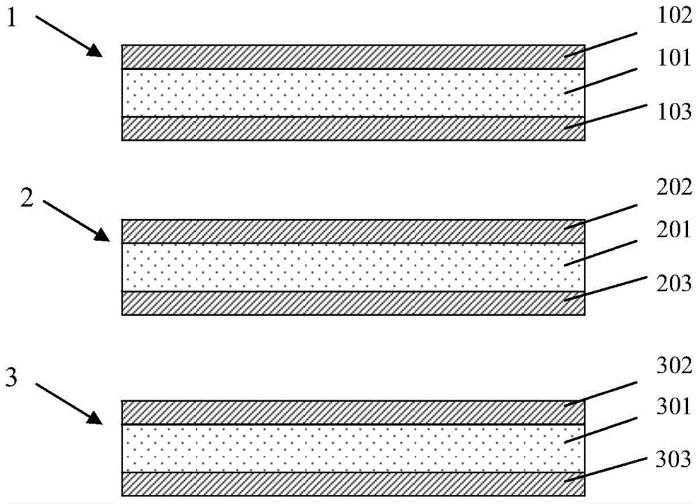
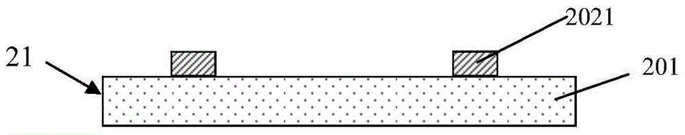
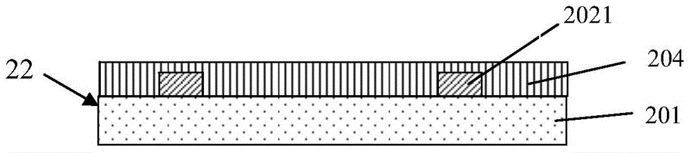
[0050] 1) Substrate production, 1, 2, and 3 are cut copper-clad laminates, copper-clad laminates 1 and 3 are used for the production of two second-layer copper layers, and the copper-clad laminate 2 located in the middle is used for the production of the optical waveguide layer. Among them, 101, 301 are dielectric layers, 102, 103, 302, 303 are copper layers, see figure 1 ; The optical waveguide substrate 21 is a copper-clad laminate that etches away most of the copper, and this substrate leaves a copper surface (copper barrier layer) 2021 in the subsequent fabrication of the optical waveguide micromirror region, see figure 2 .

[0051] 2) making the optica...


PUM


Abstract

A manufacturing method of printed circuit boards with optical waveguide couplers includes the steps of (1) manufacturing a substrate; (2) manufacturing an optical waveguide layer which is composed of a bottom coating graph, a core graph and a top coating graph; (3) manufacturing an optical waveguide reflector by coating an upper reflector on a core bevel to form a micro-mirror; (4) manufacturing the corresponding printed circuit board; (5) subjecting the printed circuit board and the substrate which is of the optical waveguide layer to the process of press fit so as to form a mixture board with the optical waveguide layer and a copper circuit layer; and (6) etching and milling to form the final optical channel. Since the graphs of the optical waveguide layer are exposed by means of gray masks and windows of the upper coating are coated with the reflector, a micro-mirror coupler is formed, and further is formed integrally with the optical waveguide couplers. The core graph comprises a core circuit and the core bevel, and the core bevel is exposed by means of gray mask. The manufacturing method has the advantages that coupling loss is low, manufacturing of the l micro-mirror is easy to achieved, and embedding density of the couplers in a light guide plate is increased.

Description

technical field [0001] The invention relates to the technical field of printed circuits, in particular to a method for manufacturing a printed circuit board containing an optical waveguide coupling device. Background technique [0002] With the development of information science and technology such as communication and computer technology, the traditional electrical interconnection of PCB copper wires will face severe challenges due to inherent problems such as LC delay and crosstalk. The industry generally believes that when the single-channel rate is above 10G, the electrical interconnection Even the technical implementation and cost will face severe challenges, requiring a new interconnection method. Optical interconnects have the distinct advantage of replacing electrical interconnects, being easier to implement and maintaining good signal integrity. The advantages of optical interconnects include: [0003] 1. The transmission loss on the optical channel is mainly dete...

Claims


Application Information

Patent Timeline
Patent Type & Authority Applications(China)
IPC IPC(8): G02B6/13G02B6/26
CPCG02B6/13G02B6/24
Inventor 严惠娟梅莉嘉.伊莫宁朱龙秀吴金华彭增时睿智
Owner SHANGHAI MEADVILLE SCI & TECH
Why Eureka
Try Eureka