Wafer positioning method

A positioning method and wafer technology, applied in the manufacture of electrical components, electrical solid devices, semiconductor/solid devices, etc., can solve the problems of difficult positioning of wafers, avoid low yield, reduce resistance value, and ensure the reliability of subsequent devices The effect formed

Inactive Publication Date: 2015-07-22
SHANGHAI HUAHONG GRACE SEMICON MFG CORP
View PDF5 Cites 8 Cited by
  • Summary
  • Abstract
  • Description
  • Claims
  • Application Information

AI Technical Summary

Problems solved by technology

[0004] The invention provides a wafer positioning method to solve the problem in the prior art that the wafer is difficult to position in the Taiko process

Method used


Image

  • Wafer positioning method

Examples


Embodiment Construction

[0018] In order to make the above objects, features and advantages of the present invention more comprehensible, specific implementations of the present invention will be described in detail below in conjunction with the accompanying drawings. It should be noted that all the drawings of the present invention are in simplified form and use inaccurate scales, and are only used to facilitate and clearly assist the purpose of illustrating the embodiments of the present invention.

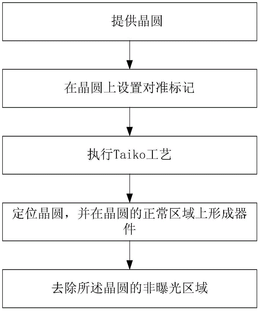
[0019] Such as figure 1 As shown, the present invention provides a wafer positioning method, specifically comprising the following steps:

[0020] Step 1: Provide a wafer, which includes a normal area and a non-exposed area. Wherein, the normal area of ​​the wafer is an area for subsequent exposure and device formation; the non-exposed area is an edge portion of the wafer, which is set around the normal area and does not need to form devices thereon. In the present invention, after the device is forme...


PUM


Abstract

The invention discloses a wafer positioning method. The wafer positioning method includes providing a wafer comprising a normal area and a non-exposure area, and setting alignment marks on the normal area and the non-exposure area respectively; implementing Taiko process; positioning the wafer and forming a device on the normal area of the wafer. By means of the Taiko process, the peripheral edge of the wafer, namely the non-exposure area, should be reserved, and the normal area and the non-exposure area of the wafer are provided with alignment marks at the same time. When the Taiko process is performed, the normal area of the wafer is ground and thinned, the alignment marks of the normal area are ground and become shallow or disappear, and the alignment marks of the non-exposure area are still reserved. Therefore, the non-exposure area is provided with the alignment marks, resistance of the semiconductor power device of an automobile electronic product can be reduced, formation of a subsequent device can be ensured, and low yield of the semiconductor power device due to the fact that the wafer is hard to position is avoided.

Description

technical field [0001] The invention relates to the field of integrated circuit manufacturing, in particular to a wafer positioning method. Background technique [0002] Semiconductor power devices (abbreviated as power devices, English: Power MOS) are semiconductor devices that perform power processing and have the ability to handle high voltage and high current. Its voltage processing range can range from tens of volts to thousands of volts. up to several thousand amps. Typical power processing includes frequency conversion processing, voltage conversion processing, flow conversion processing, power management and so on. Early semiconductor power devices include high-power diodes and thyristors, etc., which are mainly used in industry and power systems. Later, with the rapid development of new semiconductor power devices represented by power MOSFET devices, semiconductor power devices are now very widespread. In the 4C industry (Computer, Communication, Consumer Electron...

Claims


Application Information

Patent Timeline
Patent Type & Authority Applications(China)
IPC IPC(8): H01L21/02H01L23/544
CPCH01L21/02H01L23/544H01L2223/54426
Inventor 王鹏刘宇李秀莹
Owner SHANGHAI HUAHONG GRACE SEMICON MFG CORP
Why Eureka
Try Eureka