Nondestructive friction-induced nano-processing method

A technology of friction induction and nano-processing, applied in the field of nano-processing, can solve the problems of a large number of inorganic reactants being powerless, achieve the effect of shortening the etching time, simple method, and ensuring consistency

Inactive Publication Date: 2019-03-08
SOUTHWEST JIAOTONG UNIV
View PDF7 Cites 0 Cited by
  • Summary
  • Abstract
  • Description
  • Claims
  • Application Information

AI Technical Summary

Problems solved by technology

Although the above commonly used dry and wet cleaning techniques can effectively remove a small amount of organic or inorganic pollutants on the surface of single crystal silicon, they are powerless to deal with the large amount of inorganic reactants produced during the friction-induced selective etching process.

Method used


Image

  • Nondestructive friction-induced nano-processing method
  • Nondestructive friction-induced nano-processing method
  • Nondestructive friction-induced nano-processing method

Examples


Embodiment 1

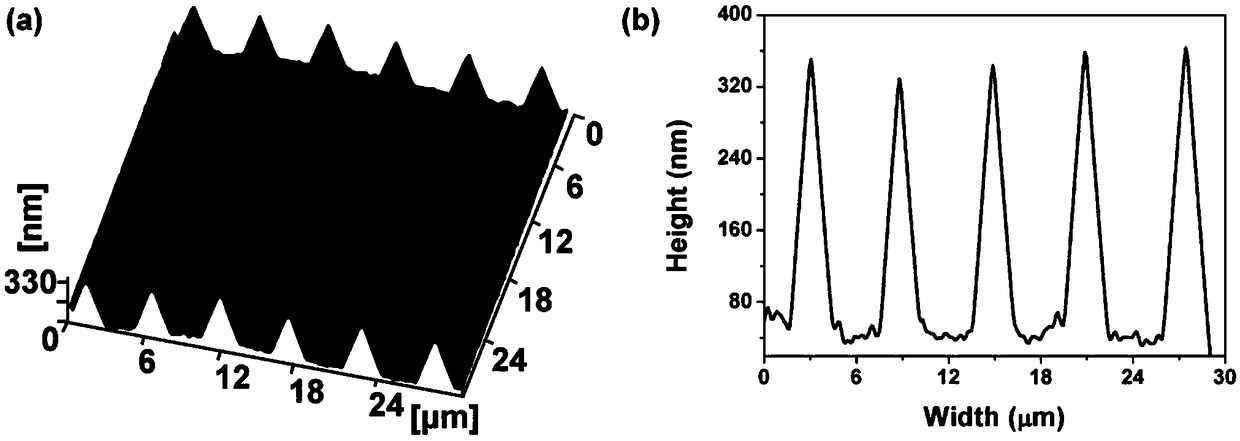
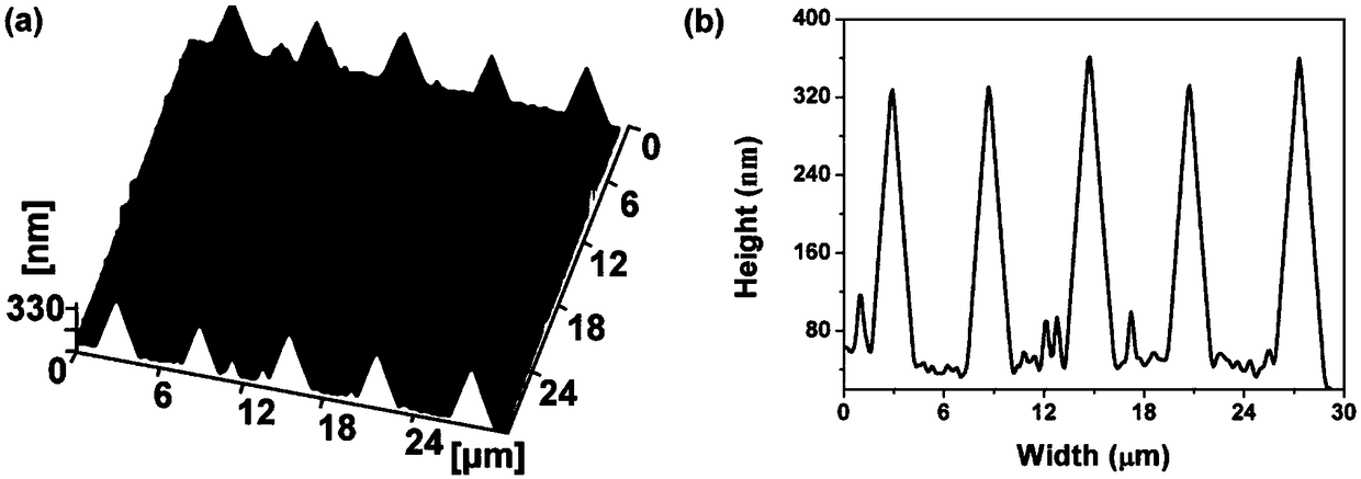
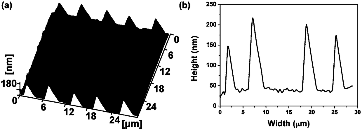
[0029] The damage-free friction-induced nanofabrication method of this embodiment includes the following steps:

[0030] S1, the monocrystalline silicon sample was ultrasonically cleaned with acetone, absolute ethanol and secondary deionized water for 5 minutes;

[0031] S2. Place the single crystal silicon sample cleaned in step S1 on a multi-probe nano-processing device, and use the diamond probe to perform scanning processing on the surface of the single crystal silicon sample according to the set processing parameters;

[0032] S3, configure a mixed solution of KOH solution and isopropanol with a mass concentration of 20%, the volume ratio of KOH solution and isopropanol is 5:1, and place the plastic beaker containing the solution in a heat-collecting magnetic stirrer The water bath is heated and kept at a constant temperature of about 25°C, and the rotational speed of the modulated rotor is 350 rpm and kept constant;

[0033] S4. Rinse the monocrystalline silicon sample ...


PUM

PropertyMeasurementUnit
heightaaaaaaaaaa
heightaaaaaaaaaa

Abstract

The invention discloses a nondestructive friction-induced nano-processing method. The method comprises the following steps: S1, cleaning the surface of a monocrystalline silicon sample to remove impurities on the surface; S2, performing scanning processing on the surface of the monocrystalline silicon sample by using a probe through a mechanical scribing processing device according to set processing parameters; S3, configuring an etching solution, placing a container containing the etching solution in a magnetic stirrer, heating in a water bath and maintaining a constant temperature, modulating the rotating speed of a rotor, and keeping the rotating speed unchanged; and S4, soaking the monocrystalline silicon sample processed in the step S2 in the container in the step S3 for etching for 10-30min after flushing the monocrystalline silicon sample, taking out the monocrystalline silicon sample, and respectively cleaning the surface of the monocrystalline silicon sample. By adoption of the method, the high-speed flow of the etching solution is kept by applying an external field in the chemical etching, so that reaction products formed on the surface of the monocrystalline silicon aretaken away quickly, the quality of a micro/nano structure on the surface of the monocrystalline silicon is ensured, meanwhile the chemical etching efficiency is accelerated, and no damage is generatedto the nano structure.

Description

technical field [0001] The invention belongs to the technical field of nano-processing, and in particular relates to a non-damaging friction-induced nano-processing method. Background technique [0002] With the continuous development of nanotechnology, micro / nano sensors and actuators exhibit excellent stability, high resolution and sensitivity, and strong anti-interference performance, and are more widely used in military and civilian fields. Among them, silicon-based micro / nanostructures are still the core of these functional devices with excellent performance. Studies have found that the pollutants on the surface of silicon-based micro / nanostructures have a greater impact on the overall performance of the device. Therefore, the effective removal of pollutants on the surface of silicon-based micro / nanostructures is becoming more and more important in the semiconductor industry. At present, the commonly used pollutant removal methods mainly include dry cleaning and wet cl...

Claims


Application Information

Patent Timeline
Patent Type & Authority Applications(China)
IPC IPC(8): B81B1/00B81C1/00
CPCB81B1/00B81B2201/02B81C1/00023B81C1/00539B81C1/00555
Inventor 钱林茂汪红波余丙军蒋淑兰陈磊江亮
Owner SOUTHWEST JIAOTONG UNIV
Why Eureka
Try Eureka