Gaas-based two-dimensional electron gas plasma oscillation method for terahertz detectors

A technology of terahertz detector and two-dimensional electron gas, which is applied in the field of ion oscillation detection of terahertz, and can solve the problems of narrow working range and so on.

Active Publication Date: 2016-08-17
INST OF SEMICONDUCTORS - CHINESE ACAD OF SCI
View PDF5 Cites 0 Cited by
  • Summary
  • Abstract
  • Description
  • Claims
  • Application Information

AI Technical Summary

Problems solved by technology

The disadvantage is a narrow working range and the need for an expensive and bulky femtosecond laser as an excitation source

Method used


Image

  • Gaas-based two-dimensional electron gas plasma oscillation method for terahertz detectors
  • Gaas-based two-dimensional electron gas plasma oscillation method for terahertz detectors
  • Gaas-based two-dimensional electron gas plasma oscillation method for terahertz detectors

Examples


Embodiment Construction

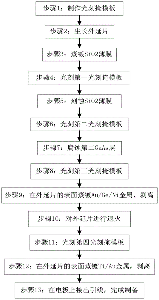
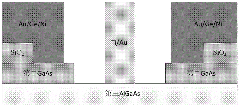
[0026] see Figure 1-Figure 3 As shown, the present invention provides a method for a GaAs-based two-dimensional electron gas plasma oscillating terahertz detector, comprising the following steps:

[0027] Step 1: Make a photolithography mask, which is a 4-version 3-inch dark-plate photolithography mask. There are four pieces in total, which are the first photolithography mask, the second photolithography mask, the third photolithography mask, the Four lithography mask templates. The photolithography mask includes a bowtie antenna, the radius of the bowtie antenna is 60-600 μm, the channel length in the photolithography mask is 500nm-11 μm, the channel width is 200nm-5 μm, and the gate length is 50nm-4 μm;

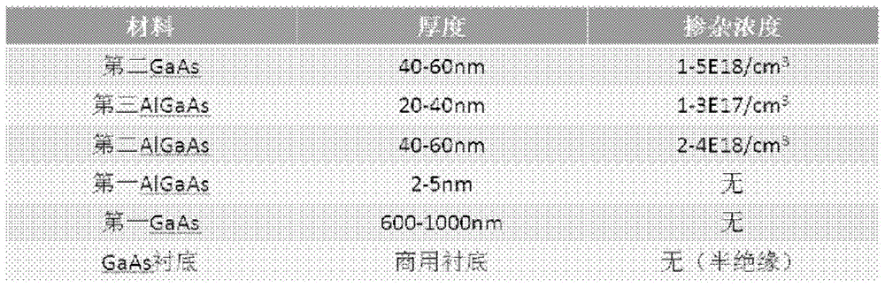
[0028] Step 2: using molecular beam epitaxy equipment to grow a GaAs layer / AlGaAs layer type channel high electron mobility device structure on the GaAs(001) substrate.

[0029] The specific steps are to sequentially grow the first GaAs layer, the first AlGaAs layer, the...


PUM


Abstract

A method for manufacturing a GaAs-based two-dimensional electron gas plasma oscillation terahertz detector includes: manufacturing four photoetching mask plates with bowtie antennas; making an epitaxial wafer on a GaAs substrate; coating a SiO2 film on the surface of the epitaxial wafer by means of evaporation; making patterns on the SiO2 film; making patterns on a second GaAs layer; etching; making patterns on the exposed second GaAs layer and the SiO2 film; evaporating Au / Ge / Ni metal, and stripping to form a source and a drain; annealing; transferring patterns of the fourth photoetching mask plate to a third AlGaAs layer with an epitaxial wafer exposed by means of photoetching; evaporating Ti / Au metal on the surface of the epitaxial wafer, and stripping to form a gate electrode on the third AlGaAs layer; leading a lead from the electrode to finish preparation. Frequency resonance range can be affected by bias voltage changes, and accordingly response gains of different frequencies can be regulated, and adjustability in response frequency is realized.

Description

technical field [0001] The invention belongs to the technical field of semiconductor materials and devices, and relates to a method for manufacturing a terahertz detector, in particular to a method for detecting terahertz on a GaAs (001) substrate by using plasma oscillation in a high electron mobility transistor. Background technique [0002] Terahertz refers to electromagnetic waves with frequencies in the range of 0.1 THz to 3 THz. In the field of terahertz technology, the emission and detection of terahertz waves is always the eternal development direction. Devices with different structures, including microradiometers, Gunn diodes, and high-ray cores, are widely used in the field of detectors, but at the same time, they also have different problems such as the need for low-temperature refrigeration and low detection rates. Terahertz detectors have increasingly widespread applications in a growing number of scientific fields. Traditional terahertz detection methods incl...

Claims


Application Information

Patent Timeline
Patent Type & Authority Patents(China)
IPC IPC(8): H01L31/119
CPCH01L31/119H01L31/1844
Inventor 徐建星査国伟张立春魏思航倪海桥贺振宏牛智川
Owner INST OF SEMICONDUCTORS - CHINESE ACAD OF SCI
Why Eureka
Try Eureka