Epitaxial structure of gallium nitride LED
A technology of light-emitting diodes and epitaxial structures, applied in electrical components, circuits, semiconductor devices, etc., can solve problems such as affecting luminous efficiency, increasing current density, and inability to completely solve them, and achieve improved luminous efficiency, average blocking effect, and uniformity of light emission. improved effect
- Summary
- Abstract
- Description
- Claims
- Application Information
AI Technical Summary
Problems solved by technology
Method used
Image


Examples
Embodiment 1
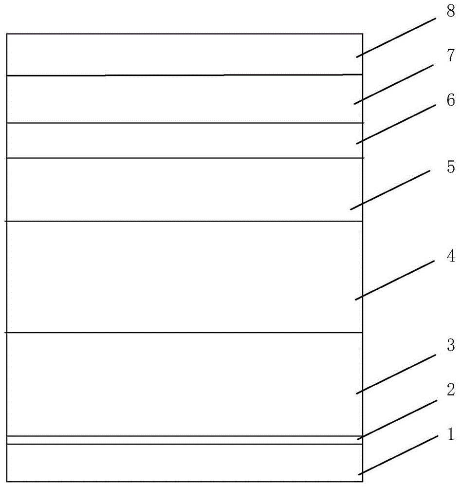
[0022] Embodiment 1 of the epitaxial structure of the gallium nitride light-emitting diode is as figure 1 As shown, it includes sapphire substrate 1, gallium nitride two-dimensional crystal layer 2, non-doped gallium nitride layer 3, N-type gallium nitride doped layer 4, 5 periods of lower quantum well structure 5, 2 periods The buffer insertion layer 6, the upper quantum well structure 7 of 4 periods and the P-type gallium nitride doped layer 8.
[0023] The lower quantum well structure 5 of this example is as figure 2 As shown, there are 5 periods, and each period includes a gallium nitride barrier layer 51 and an indium gallium nitride well layer 52 . Each period of the upper quantum well structure 7 is the same as each period of the lower quantum well structure 5 .
[0024] The buffer insert layer 6 in this example is as image 3 As shown, there are 2 periods, and the buffer insertion layer of each period includes a P-type gallium nitride doped layer 61, a P-type indiu...
Embodiment 2
[0029] For ease of comparison, the substrate 1, gallium nitride two-dimensional crystal layer 2, non-doped gallium nitride layer 3, N-type gallium nitride doped layer 4 and P-type gallium nitride doped layer 8 of this example are the same as those in the embodiment 1 is the same.
[0030] The lower quantum well structure 5 of this example is 4 periods, each period includes a gallium nitride barrier layer 51 and an indium gallium nitride well layer 52, the upper quantum well structure 7 is 1 period, and the lower quantum well structure A cycle is the same.
[0031] The buffer insertion layer 6 in this example is one period, including a P-type GaN doped layer 61 , a P-type InGaN doped layer 62 and an N-type GaN doped layer 63 .
[0032] Wherein the P-type gallium nitride doped layer 61 has a thickness of 50nm, is doped with magnesium Mg, and has a doping concentration of 50×10 17 / cm 3 ;
[0033] In this example, a P-type InGaN doped layer 62 of the buffer insertion layer 6 ...
Embodiment 3
[0037] The substrate 1 , gallium nitride two-dimensional crystal layer 2 , non-doped gallium nitride layer 3 , n-type gallium nitride doped layer 4 and p-type gallium nitride doped layer 8 in this example are the same as those in the first embodiment.
[0038] The lower quantum well structure 5 of this example is 10 periods, and each period includes a gallium nitride barrier layer 51 and an indium gallium nitride well layer 52, and the upper quantum well structure 7 is 8 periods, and each period is connected with the lower quantum well structure. One period of the well structure 5 is the same.
[0039] The buffer insertion layer 6 in this example has three periods, and each period includes a P-type GaN doped layer 61 , a P-type InGaN doped layer 62 and an N-type GaN doped layer 63 . Each cycle of the buffer insertion layer 6 is the same.
[0040] Wherein the P-type gallium nitride doped layer 61 has a thickness of 30 nm, is doped with magnesium Mg, and has a doping concentrat...
PUM
 Abstract
Description
Claims
Application Information
 - R&D
- Intellectual Property
- Life Sciences
- Materials
- Tech Scout
- Unparalleled Data Quality
- Higher Quality Content
- 60% Fewer Hallucinations
Browse by: Latest US Patents, China's latest patents, Technical Efficacy Thesaurus, Application Domain, Technology Topic, Popular Technical Reports.
© 2025 PatSnap. All rights reserved.Legal|Privacy policy|Modern Slavery Act Transparency Statement|Sitemap|About US| Contact US: help@patsnap.com