P-type silicon microchannel based surface uniform nano modification method

A technology with a uniform surface and silicon microchannels, applied in the fields of nanotechnology, nanotechnology, nanotechnology, etc. for materials and surface science, can solve the problems of irregular shape, large particle size, complex process, etc., and achieve low production costs. , The effect of high particle purity and good dispersibility

Active Publication Date: 2015-08-12
EAST CHINA NORMAL UNIVERSITY +1
View PDF1 Cites 2 Cited by
  • Summary
  • Abstract
  • Description
  • Claims
  • Application Information

AI Technical Summary

Problems solved by technology

However, there are unavoidable disadvantages of high temperature, high energy consumption, and complicated process in solid-state reaction, and the prepared particles are large in size and irregular in shape.

Method used


Image

  • P-type silicon microchannel based surface uniform nano modification method
  • P-type silicon microchannel based surface uniform nano modification method
  • P-type silicon microchannel based surface uniform nano modification method

Examples


Embodiment 1

[0041] 1) Configure electroless nickel plating solution, the composition of the solution includes 2mol / L NiCl 2 ·6H 2 O, 2mol / L Na 2 HPO 4 ·7H 2 O, 2mol / L NH 4 Cl.

[0042] 2) Drop the solution prepared in step 1) into a certain amount of ammonia water to adjust the pH value of the solution so that the pH value is 9.

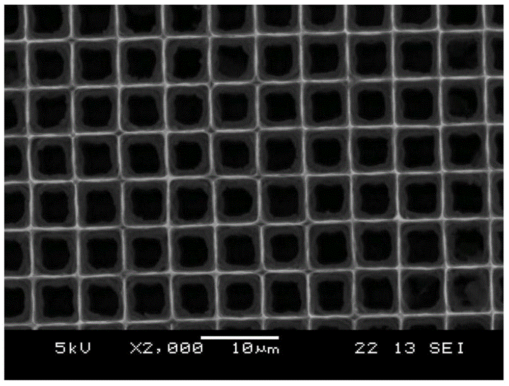
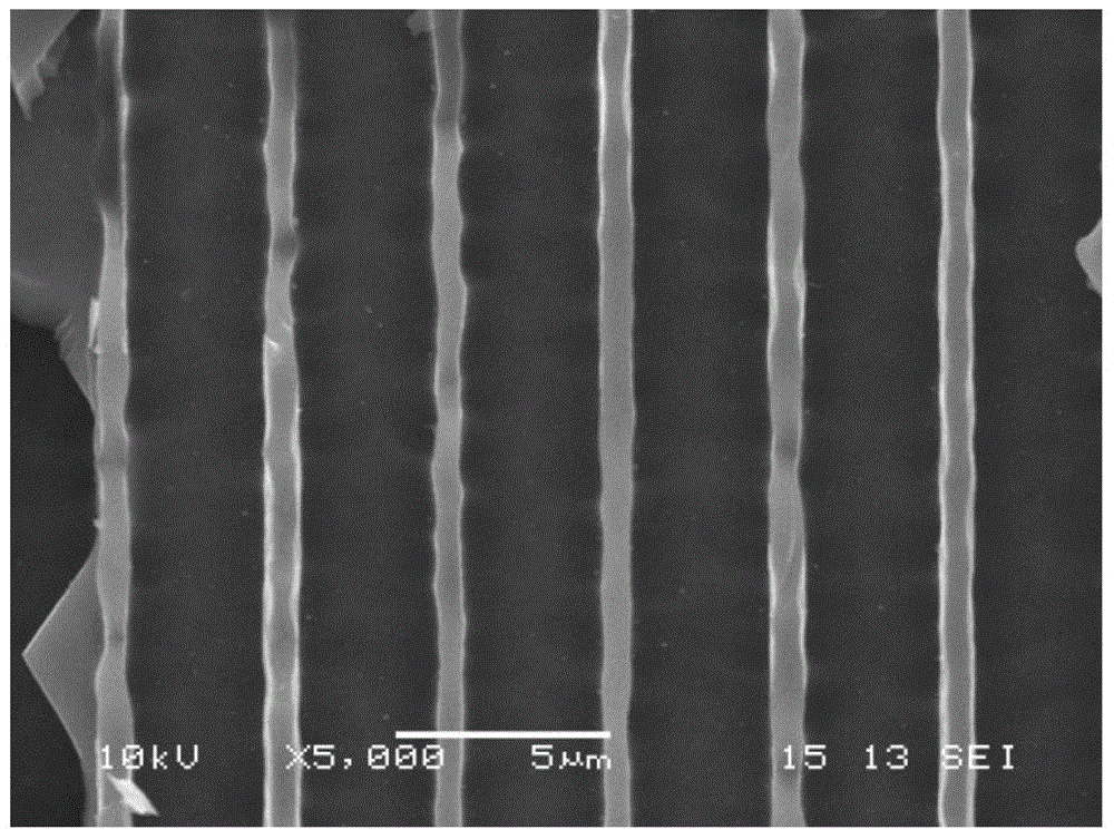
[0043] 3) Put the electroplating solution after adjusting the pH in step 2) into a water bath and heat it to 90°C, put the silicon microchannel plate cleaned in 1 into and keep it for 40 minutes. The surface morphology of the obtained sample is as Figure 2a , 2b ;by Figure 2a And it can be seen that nickel is uniformly covered on the surface of the microchannel; Figure 2b It can be seen that nickel is uniformly covered inside the microchannel.

[0044] 4) The sample of step 3) electrolessly deposited nickel is electrochemically deposited with a nickel layer to enhance the conductivity of the sample, and the deposition solution contains 2mol / L Ni(NO 3 ) 2 ·6H 2 Mixtu...

Embodiment 2

[0047] 1) Configure an electroless nickel plating solution, the composition of the solution includes 0.1mol / L NiCl 2 ·6H 2 O, 0.1mol / L Na 2 HPO 4 ·7H 2 O, 0.1mol / L NH 4 Cl.

[0048] 2) Drop the solution prepared in step 1) into a certain amount of ammonia water to adjust the pH value of the solution so that the pH value is 7.

[0049] 3) Put the electroplating solution whose pH value has been adjusted in step 2) into a water bath and heat it to 50°C, put the silicon microchannel plate cleaned in 1 into and keep it for 10 minutes. The surface morphology of the obtained sample is as Figure 2a , 2b ;by Figure 2a And it can be seen that nickel is uniformly covered on the surface of the microchannel; Figure 2b It can be seen that nickel is uniformly covered inside the microchannel.

[0050] 4) The sample of step 3) electrolessly deposited nickel is electrochemically deposited with a nickel layer to enhance the conductivity of the sample. The deposition solution contains 0.05mol / L Ni(NO...

Embodiment 3

[0053] 1) Configure an electroless nickel plating solution, the composition of the solution includes 1mol / L NiCl 2 ·6H 2 O, 1mol / L Na 2 HPO 4 ·7H 2 O, 1.5mol / L NH 4 Cl.

[0054] 2) Drop the solution prepared in step 1) into a certain amount of ammonia water to adjust the pH value of the solution to make its pH value 8.

[0055] 3) Put the electroplating solution whose pH value has been adjusted in step 2) into a water bath and heat it to 70°C, put the silicon microchannel plate cleaned in 1 into and keep it for 30 minutes. The surface morphology of the obtained sample is as Figure 2a , 2b ;by Figure 2a And it can be seen that nickel is uniformly covered on the surface of the microchannel; Figure 2b It can be seen that nickel is uniformly covered inside the microchannel.

[0056] 4) Electrochemically deposit a nickel layer on the sample of step 3) electrolessly deposited nickel to enhance the conductivity of the sample. The deposition solution is containing 1mol / L Ni(NO 3 ) 2 ·6H 2...


PUM


Abstract

The invention relates to the technical field of nano-grade material and microstructure, and discloses a method for uniformly growing a nanostructured material on a uniform chemically nickel-plated silicon microchannel substrate structure. The method comprises the following steps: silicon microchannels with a needed shape and separated from a silicon substrate are cut with laser; a uniform nickel conductive layer is grown on the surfaces of the microchannels with a chemical nickel-plating method; a nickel deposition time is adjusted, such that the resistance of the nickel-plated silicon microchannels is lower than 2ohm; a layer of nanostructure is grown on the surfaces of the nickel-plated microchannels with a hydrothermal method, wherein the nanostructure is composed of a composite metal oxide CoMoO4. According to the invention, the nanostructure is grown on the surfaces and insides of the nickel-plated silicon microchannels with micron-grade pore sizes with the hydrothermal method, such that the uniformity and stability of the structure are improved, and a problem of severe microchannel blockage caused by physically delivering materials to the inner sides of the microchannels is avoided. The material has good electrochemical activity, and has certain potential to be used in the field of new energy.

Description

Technical field [0001] The invention belongs to the technical field of micro-electromechanical systems, and specifically relates to a method based on uniform nano-modification of the surface of a p-type silicon microchannel. Background technique [0002] Nano-modification has been a subject of extensive research in materials science in the past few decades. Its characteristic is to make a layer of modified materials with nano-scale on silicon, metal surfaces, metal oxides, carbon layers and other surfaces. This modified layer has a wide range of applications, including lithium-ion batteries, sensors, super capacitors, etc. The production of nanomaterials greatly improves the specific surface area of ​​the active material deposited on the surface of the nanomaterial, and the efficiency of the active material is fully utilized, thereby improving the performance of the device. So far, most nanomaterials are built on irregular structures, such as nickel foam, carbon cloth, and even ...

Claims


Application Information

Patent Timeline
IPC IPC(8): B82B3/00B82Y30/00B82Y40/00C23C18/36C25D3/12
Inventor 王连卫李劢徐少辉朱一平
Owner EAST CHINA NORMAL UNIVERSITY
Why Eureka
Try Eureka