
GaN schottky diode with hanging beam lead structure and manufacturing method thereof

A Schottky diode and beam lead technology, which is applied in semiconductor/solid-state device manufacturing, electrical components, electrical solid-state devices, etc., can solve the problems of difficulty in the preparation of suspended beam leads, chemical corrosion and dry etching cannot be realized, etc. , to achieve the effect of improving work efficiency and device quality, reducing trouble, and reducing assembly difficulty

Active Publication Date: 2015-08-19
THE 13TH RES INST OF CHINA ELECTRONICS TECH GRP CORP
View PDF6 Cites 14 Cited by
  • Summary
  • Abstract
  • Description
  • Claims
  • Application Information

AI Technical Summary

Problems solved by technology

Since GaN and the substrate above 50um cannot be realized by chemical etching or dry etching, it is difficult to prepare the suspended beam lead of the Schottky diode device. At present, there is no GaN Schottky diode with beam lead.

Method used


Image

  • GaN schottky diode with hanging beam lead structure and manufacturing method thereof
  • GaN schottky diode with hanging beam lead structure and manufacturing method thereof

Examples


Embodiment Construction

[0029] The technical solutions in the embodiments of the present invention are clearly and completely described below in conjunction with the accompanying drawings in the embodiments of the present invention. Obviously, the described embodiments are only part of the embodiments of the present invention, not all of them. Based on the embodiments of the present invention, all other embodiments obtained by persons of ordinary skill in the art without making creative efforts belong to the protection scope of the present invention.

[0030] In the following description, a lot of specific details are set forth in order to fully understand the present invention, but the present invention can also be implemented in other ways different from those described here, and those skilled in the art can do it without departing from the meaning of the present invention. By analogy, the present invention is therefore not limited to the specific examples disclosed below.

[0031] like Figure 1-...


PUM


Abstract

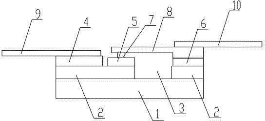
The invention discloses a GaN schottky diode with a hanging beam lead structure and a manufacturing method thereof and relates to the technical field of semiconductor devices and manufacturing methods thereof. The diode comprises a substrate. The substrate is provided with N+ GaN layers and an N- GaN layer. A first ohmic contact layer and the N- GaN layer are arranged at an interval. An upper surface of the right highly-doped N+ GaN layer is provided with a second ohmic contact layer. An upper surface of the N- GaN layer is provided with a schottky contact layer. The schottky contact layer and the second ohmic contact layer are connected through an air bridge. The first ohmic contact layer is provided with a first handing beam lead. The air bridge is provided with a second hanging beam lead. The diode utilizes the beam lead structure, achieves the press welder assembly of a miniature chip, reduces trouble caused by conductive tape coating, reduces the device assembly difficulty, and improves the working efficiency and the device quality.

Description

technical field [0001] The invention relates to the technical field of semiconductor devices and manufacturing methods thereof, in particular to a GaN Schottky diode with a suspended beam lead structure and a manufacturing method thereof. Background technique [0002] Schottky frequency doubler diode devices based on traditional semiconductor materials such as Si and GaAs are limited by the properties of the material itself, so it is difficult to further improve the corresponding indicators such as power and breakdown voltage. In recent years, a new generation of wide-bandgap semiconductor materials represented by group III nitrides has developed rapidly. It has excellent material properties such as wide band gap, high saturated electron drift velocity, high breakdown field strength and high thermal conductivity, and has great development potential in the field of millimeter wave and submillimeter wave high-power electronic devices. Research on GaN-based Schottky diode mill...

Claims


Application Information

Patent Timeline
IPC IPC(8): H01L23/49H01L29/872H01L21/329
Inventor 梁士雄房玉龙邢东王俊龙杨大宝张立森冯志红
Owner THE 13TH RES INST OF CHINA ELECTRONICS TECH GRP CORP
Learn More