TFT substrate structure manufacturing method and TFT substrate structure thereof

A manufacturing method and substrate technology, which are applied in semiconductor/solid-state device manufacturing, semiconductor devices, electrical components, etc., can solve problems such as large costs and expenses, and achieve the effects of reducing production costs, saving processes, and improving production efficiency.

Inactive Publication Date: 2015-09-09
WUHAN CHINA STAR OPTOELECTRONICS TECH CO LTD
View PDF4 Cites 9 Cited by
  • Summary
  • Abstract
  • Description
  • Claims
  • Application Information

AI Technical Summary

Problems solved by technology

But this means that a separate photomask design and a photolithography process need to be carried out for the fabrication of the n-type lightly doped region 320, which requires a lot of cost

Method used


Image

  • TFT substrate structure manufacturing method and TFT substrate structure thereof
  • TFT substrate structure manufacturing method and TFT substrate structure thereof
  • TFT substrate structure manufacturing method and TFT substrate structure thereof

Examples


Embodiment Construction

[0037] In order to further illustrate the technical means adopted by the present invention and its effects, the following describes in detail in conjunction with preferred embodiments of the present invention and accompanying drawings.

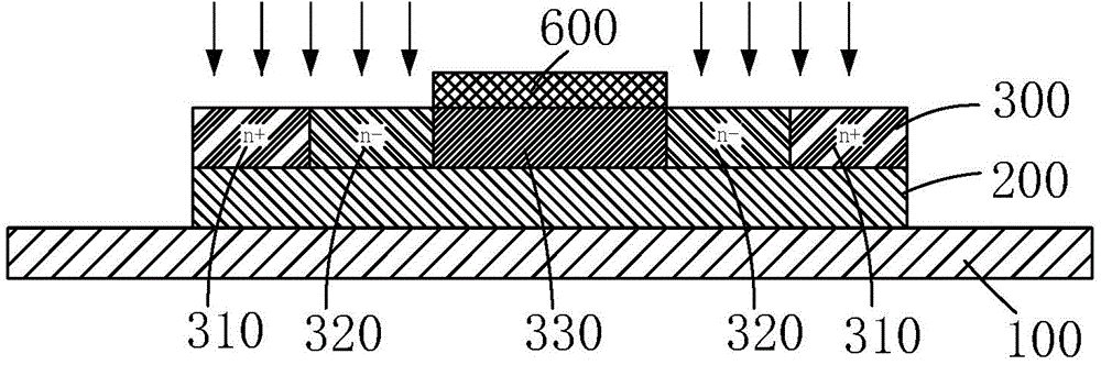
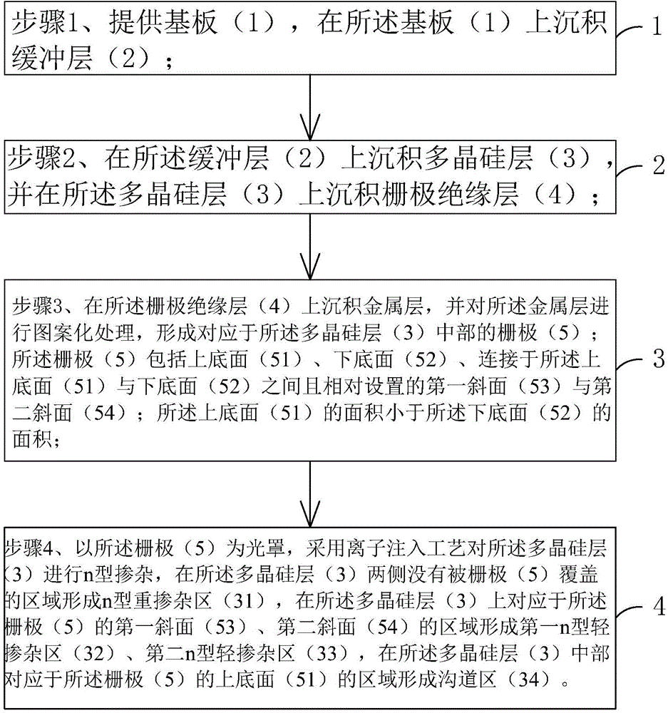
[0038] see figure 2 , the present invention at first provides a kind of manufacturing method of TFT substrate structure, comprises the following steps:

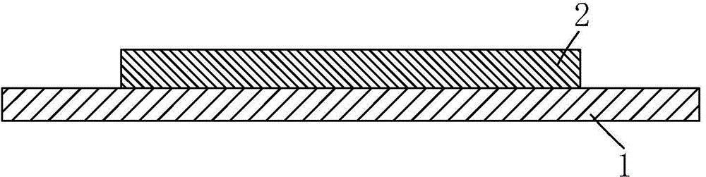
[0039] Step 1, such as image 3 As shown, a substrate 1 is provided on which a buffer layer 2 is deposited.

[0040] Specifically, the substrate 1 may be a glass substrate or a plastic substrate, and the material of the buffer layer 2 may be silicon oxide (SiOx), silicon nitride (SiNx), or a combination of the two.

[0041] Step 2, such as Figure 4 As shown, a polysilicon (Poly-Si) layer 3 is deposited on the buffer layer 2 , and a gate insulating layer 4 is deposited on the polysilicon layer 3 .

[0042] Specifically, the material of the gate insulating layer 4 may be silicon oxide, si...


PUM


Abstract

The invention provides a TFT substrate manufacturing method and a TFT substrate structure thereof. According to the TFT substrate structure manufacturing method, through an etching parameter in manufacturing a gate, oblique surfaces are formed at two sides of the gate. Furthermore the gate is used as an optical cover. Ion implantation is performed on a polysilicon layer. Simultaneously n-type heavily doped regions and n-type lightly doped regions are formed on the polysilicon layer. The TFT substrate manufacturing method and the TFT substrate structure have functions of enlarging a resistance, dispersing a strong electric field next to electrodes, preventing device characteristic reduction by a hot carrier effect caused by existence of a partial strong electric field, saving a process for singly forming the n-type lightly doped region, improving generation efficiency and reducing production cost. According to the TFT substrate structure, the polysilicon layer comprises the n-type heavily doped regions at two sides and the n-type lightly doped regions between the channel region of the polysilicon layer and the n-type heavily doped regions, thereby preventing generation of the partial strong electric field, and eliminating the effect of a hot carrier to the characteristic of the device.

Description

technical field [0001] The invention relates to the field of display technology, in particular to a method for manufacturing a TFT substrate structure and the TFT substrate structure. Background technique [0002] Liquid crystal display (Liquid Crystal Display, LCD) has many advantages such as thin body, power saving, no radiation, etc., and has been widely used, such as: mobile phone, personal digital assistant (PDA), digital camera, computer screen or notebook computer screen etc. [0003] Generally, a liquid crystal display device includes a housing, a liquid crystal panel disposed in the housing, and a backlight module disposed in the housing. Among them, the structure of the liquid crystal panel is mainly composed of a thin film transistor array substrate (Thin Film Transistor Array Substrate, TFT Array Substrate), a color filter substrate (Color Filter, CF), and a liquid crystal layer (Liquid Crystal) disposed between the two substrates. Crystal Layer), its working p...

Claims


Application Information

Patent Timeline
Patent Type & Authority Applications(China)
IPC IPC(8): H01L29/786H01L21/336H01L29/423H01L29/16H01L27/12
CPCH01L27/1214H01L29/16H01L29/42376H01L29/66742H01L29/786H01L29/78627H01L29/42384H01L29/518H01L29/66598H01L29/66757H01L29/78621H01L29/78675H01L29/78696H01L27/1222H01L27/127H01L29/4908H01L29/51
Inventor 郭文帅明星申智渊
Owner WUHAN CHINA STAR OPTOELECTRONICS TECH CO LTD
Why Eureka
Try Eureka