III-V clan nano wire planar transistor based on SOI substrate and preparation method thereof

A nanowire and transistor technology, applied in the field of III-V nanowire planar transistors and their preparation, can solve problems such as unfavorable preparation, and achieve the effects of eliminating rectification effect, facilitating integration, and simple device preparation process

Inactive Publication Date: 2015-09-23
INST OF SEMICONDUCTORS - CHINESE ACAD OF SCI
View PDF5 Cites 7 Cited by
  • Summary
  • Abstract
  • Description
  • Claims
  • Application Information

AI Technical Summary

Problems solved by technology

In order to facilitate the logic wiring of the gate and the preparation of the planar process, a horizontal nanowire structure is usually required, but the vertical nanowire structure needs to be artificially transferred to obtain a horizontal structure, such as ultrasonic vibration of the vertical nanowire in a high-concentration ethanol solution , the shaken-off nanowires also need to use electron beam exposure and other methods to position the electrodes, which is not conducive to the preparation of large areas

Method used


Image

  • III-V clan nano wire planar transistor based on SOI substrate and preparation method thereof
  • III-V clan nano wire planar transistor based on SOI substrate and preparation method thereof
  • III-V clan nano wire planar transistor based on SOI substrate and preparation method thereof

Examples


Embodiment Construction

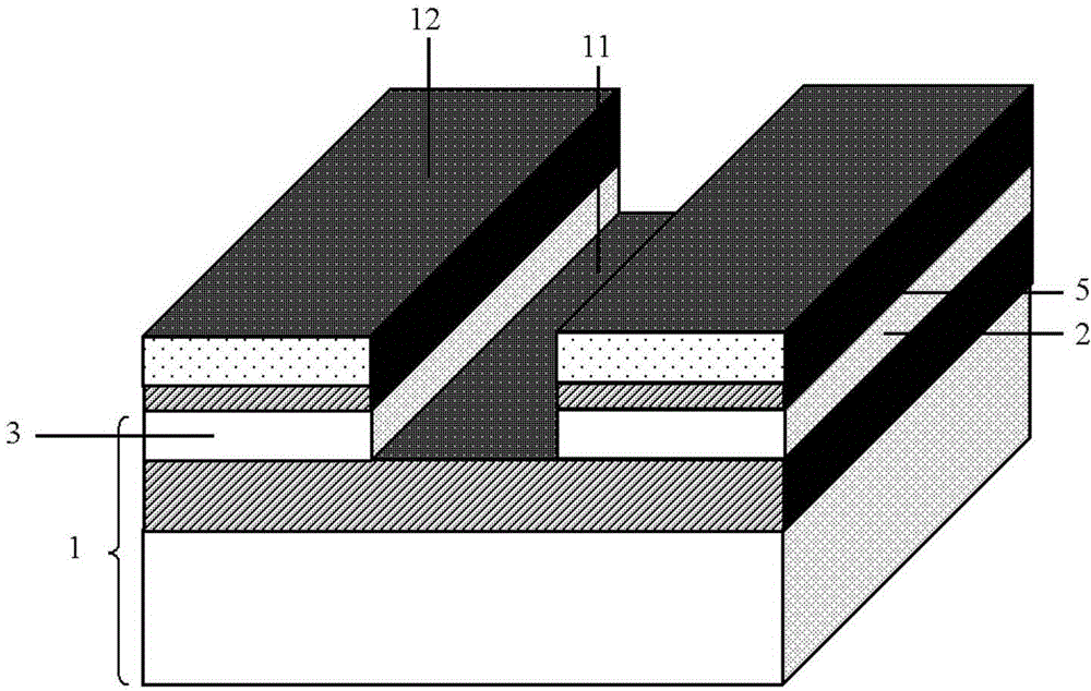
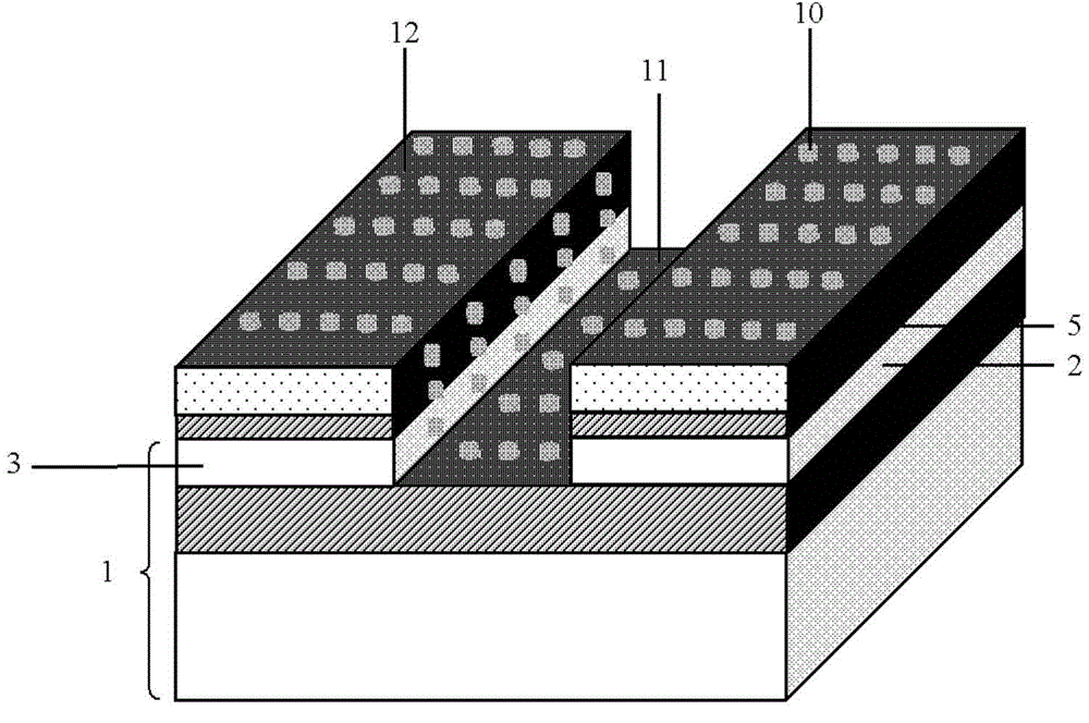
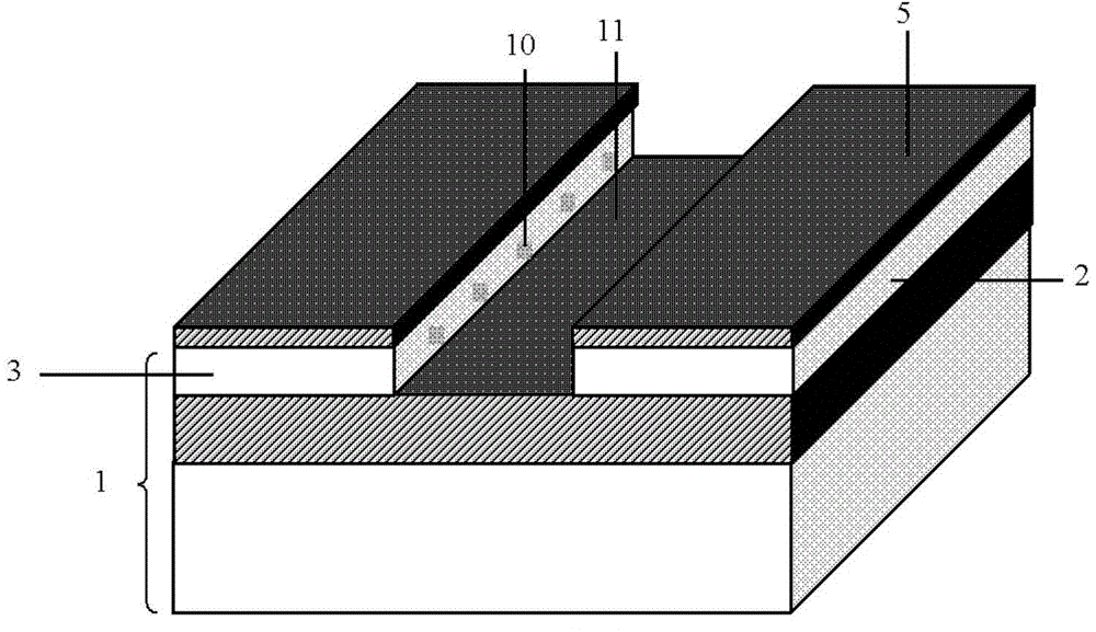
[0039] see Figure 1-Figure 5 As shown, the present invention provides a kind of III-V family nanowire planar transistor based on SOI substrate, comprising:

[0040] An SOI substrate 1, wherein the top layer silicon of the SOI substrate 1 is a (110) crystal plane, and the thickness is 88nm;

[0041] A source region 2 and a drain region 3, the source region 2 and the drain region 3 are formed on the SOI substrate 1, wherein the silicon crystal planes of the side walls of the source region 2 and the drain region 3 are {111} crystal planes, and the doping type It is N-type with a doping concentration of 10 18 -10 19 cm -3 , the ion implantation junction depth is 17-100nm;

[0042] A plurality of III-V group nanowires 4, the plurality of III-V group nanowires 4 connect the source region 2 and the drain region 3 to form a conductive channel, wherein the plurality of III-V group nanowires 4 can be In x Ga 1-x As(0≤x≤1), GaP, GaN or InP materials, the high electron mobility of ...


PUM

PropertyMeasurementUnit
thicknessaaaaaaaaaa
thicknessaaaaaaaaaa
diameteraaaaaaaaaa

Abstract

An III-V clan nano wire planar transistor based on a SOI substrate and a preparation method thereof; the transistor comprises the following elements: the SOI substrate; a source zone and a drain zone formed on the SOI substrate; a plurality of III-V clan nano wires connected with the source zone and the drain zone; a SiO2 buffer layer formed on surfaces of the source zone and the drain zone; an insulation medium layer formed on surfaces of the III-V clan nano wires and the SiO2 buffer layer, and completely wrapping the III-V clan nano wires; a source electrode formed on the top of the soruce zone; a drain electrode formed on the top of the drain zone; a grid electrode formed on the plurality of III-V clan nano wires between the source zone and the drain zone, and wrapping the plurality of III-V clan nano wires. The preparation of plane nano wire transistors can be realized.

Description

technical field [0001] The invention relates to the technical field of manufacturing semiconductor devices, in particular to a III-V group nanowire planar transistor based on an SOI substrate and a preparation method thereof. Background technique [0002] Silicon-based III-V transistors can use higher mobility to obtain higher drive current at lower drive voltage, making their processing speed three times higher than before, or reducing their power consumption to 1 / 10 of the original, This is conducive to the acquisition of high frequency, low power consumption devices. However, due to the lattice mismatch, thermal expansion coefficient mismatch and crystal structure difference between silicon and III-V materials, the resulting dislocations make the heterogeneous integration of the two difficult. By vertically growing III-V nanowires, the contact area with silicon can be reduced, and the nanowires can release the lattice mismatch stress and thermal mismatch from the two dim...

Claims


Application Information

Patent Timeline
Patent Type & Authority Applications(China)
IPC IPC(8): H01L29/78H01L29/10H01L29/06H01L21/762H01L21/02H01L29/66B82Y40/00
CPCH01L29/78B82Y40/00H01L21/02488H01L21/7624H01L29/0684H01L29/1033H01L29/66469
Inventor 洪文婷韩伟华吕奇峰杨富华
Owner INST OF SEMICONDUCTORS - CHINESE ACAD OF SCI
Why Eureka
Try Eureka