Supercharge Your Innovation With Domain-Expert AI Agents!

Method for preparing nickel silicide

A technology of nickel silicide and metal silicide, applied in semiconductor/solid-state device manufacturing, electrical components, circuits, etc., can solve the adjustment of NMOS and PMOS, without considering how to meet the requirements of different devices, without considering the negative side of TiN stress layer Function and other issues to achieve the effect of avoiding damage and improving performance

Active Publication Date: 2015-09-30
SHANGHAI HUALI MICROELECTRONICS CORP
View PDF3 Cites 0 Cited by
  • Summary
  • Abstract
  • Description
  • Claims
  • Application Information

AI Technical Summary

Problems solved by technology

[0006] However, the above-mentioned existing Ni silicide formation process does not adjust NMOS and PMOS respectively, and adopts TiN with a single stress to cover the NMOS and PMOS as a protective layer of NiPt, and a single stress (tensile stress or compressive stress) Stress) TiN can only contribute to the improvement of electron mobility or hole mobility of one of NMOS or PMOS, but in the case of benefiting one of them, it will be detrimental to the electrical performance of the other device influences
In addition, depositing NiPt metal layers with the same thickness and Pt content on NMOS and PMOS devices does not take into account how to meet the requirements of different devices
[0007] Therefore, the existing Ni silicide formation process does not take into account the negative effects brought by the TiN stress layer introduced during the formation of metal silicide, and how to meet the requirements of different devices, it needs to be optimized

Method used


Image

  • Method for preparing nickel silicide
  • Method for preparing nickel silicide
  • Method for preparing nickel silicide

Examples


Embodiment Construction

[0029] The specific embodiment of the present invention will be further described in detail below in conjunction with the accompanying drawings.

[0030] It should be noted that, in the following specific embodiments, when describing the embodiments of the present invention in detail, in order to clearly show the structure of the present invention for the convenience of description, the structures in the drawings are not drawn according to the general scale, and are drawn Partial magnification, deformation and simplification are included, therefore, it should be avoided to be interpreted as a limitation of the present invention.

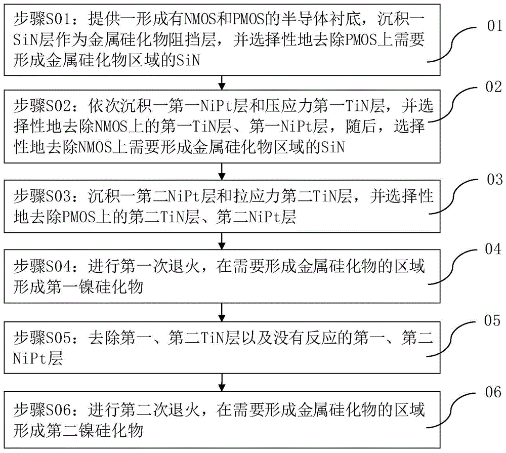
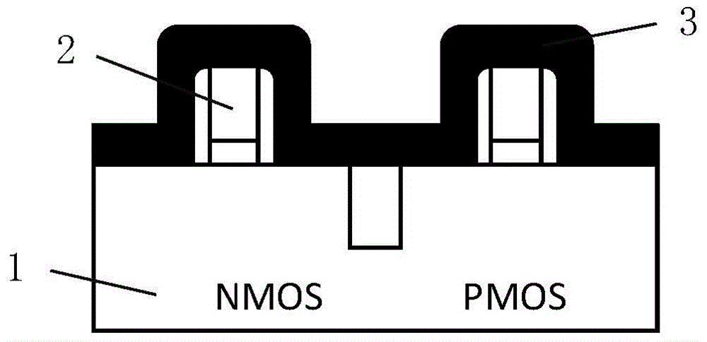
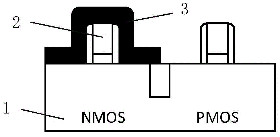
[0031] In the following specific embodiments of the present invention, please refer to figure 1 , figure 1 It is a flowchart of a method for making nickel silicide in the present invention. Also, see Figure 2 to Figure 7 , Figure 2 to Figure 7 is a preferred embodiment of the present invention according to figure 1 Schematic diagram of the pro...


PUM

PropertyMeasurementUnit
thicknessaaaaaaaaaa
thicknessaaaaaaaaaa

Abstract

The invention discloses a method for preparing nickel silicide. TiN layers with opposite stress are deposited on an NMOS (N-channel metal oxide semiconductor) and a PMOS (P-channel metal oxide semiconductor) to serve as cap layers of NiPt; different stresses are memorized after reaction and phase change in the follow-up nickel silicide formation process, so that the formed nickel silicide can apply pull stress to NMOS channels and PMOS channels, negative effects caused by introduction of the stress layers are avoided in the formation process of metal silicide, and the performance of devices is improved; NiPt covering the NMOS and the PMOS contains Pt with different content and can meet different requirements of the devices; besides, the SiN reserved on the NMOS can be used for removing NiPt on the NMOS, and additional damage to S / D (source / drain) is avoided.

Description

technical field [0001] The invention relates to the technical field of semiconductor integrated circuit manufacturing, and more specifically, to a method for making nickel silicide. Background technique [0002] In semiconductor manufacturing technology, metal silicide is widely used in source / drain contacts and gate contacts to reduce contact resistance due to its low resistivity and good adhesion with other materials. Metals with high melting points such as Ti, Co, Ni, etc. can react with silicon to form metal silicides with low resistivity through one-step or multi-step annealing process. With the continuous improvement of the semiconductor process level, especially at the technology node of 45nm and below, in order to obtain lower contact resistance, nickel and nickel alloys (such as NiPt) have become the main materials for forming metal silicides. [0003] As the miniaturization of the feature size of VLSI continues, the size of field effect transistors is also getting...

Claims


Application Information

Patent Timeline
Patent Type & Authority Applications(China)
IPC IPC(8): H01L21/8238H01L21/28H01L29/78
CPCH01L21/28518H01L21/823871H01L29/7845
Inventor 鲍宇
Owner SHANGHAI HUALI MICROELECTRONICS CORP
Features
  • R&D
  • Intellectual Property
  • Life Sciences
  • Materials
  • Tech Scout
  • Unparalleled Data Quality
  • Higher Quality Content
  • 60% Fewer Hallucinations
Learn More