Method for preparing silicon quantum dot films through microwave annealing

A technology of microwave annealing and silicon quantum dots, which can be used in final product manufacturing, sustainable manufacturing/processing, photovoltaic power generation, etc. It can solve problems such as silicon quantum dots that have not yet been seen, and achieve lower crystallization temperature, faster separation, and lower costs. Effect

Inactive Publication Date: 2015-09-30
YUNNAN NORMAL UNIV
View PDF3 Cites 2 Cited by
  • Summary
  • Abstract
  • Description
  • Claims
  • Application Information

AI Technical Summary

Problems solved by technology

Further search and analysis of the literature has not yet seen a new method for preparing silicon

Method used


Image

  • Method for preparing silicon quantum dot films through microwave annealing
  • Method for preparing silicon quantum dot films through microwave annealing
  • Method for preparing silicon quantum dot films through microwave annealing

Examples


Embodiment 1

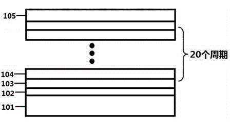
[0024] Si / SiO x Preparation of multilayer films

[0025] Step 1. Substrate cleaning: A quartz plate with a thickness of 1mm is ultrasonically cleaned by deionized water, acetone, absolute ethanol and deionized water for 15 minutes;

[0026] Step 2. Sputtering coating: prepare SiO on the quartz substrate by magnetron co-sputtering x / Si multilayer film. Background vacuum 5×10 -5 Pa, the substrate temperature is 300°C, the argon gas flow rate is 40sccm, the working pressure is 0.3Pa, the pulse power of the Si target is 100W, and the SiO is connected 2 The RF power of the target is 40W. Such as figure 1 As shown, a layer of SiO with a thickness of 10 nm is grown on the substrate 101 2 buffer layer 102, and then alternately grow a 5nm-thick silicon-rich silicon oxide layer 103 and a 5nm-thick silicon layer 104 (a total of 20 cycles), and finally grow a layer of 10nm-thick SiO 2 Capping layer 105;

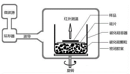
[0027] Microwave annealing crystallization process

[0028] Take out the s...

Embodiment 2

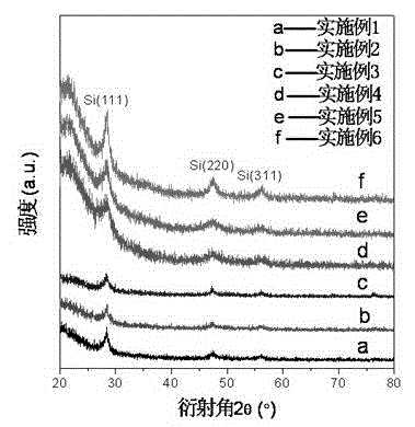
[0030] Similar to Example 1, the difference is that the annealing temperature is 800°C. The GIXRD test result of the silicon quantum dot obtained is as follows image 3 (b) shown.

Embodiment 3

[0032] Similar to Example 1, the difference is that the annealing temperature is 700°C. The GIXRD test result of the silicon quantum dot obtained is as follows image 3 (c) shown.


PUM

PropertyMeasurementUnit
Thicknessaaaaaaaaaa
Thicknessaaaaaaaaaa
Thicknessaaaaaaaaaa

Abstract

The invention relates to a method for preparing silicon quantum dot films through microwave annealing. Specifically, magnetron-sputtering-deposited silicon-rich silicide films are placed in a microwave annealing furnace for annealing at the lower temperature, and the uniform silicon quantum dot films are prepared. The method is good in controllability, high in repeatability, simple, effective and high in operability due to adoption of reliable magnetron co-sputtering and microwave annealing technologies. According to the main technical scheme, the method comprises steps as follows: firstly, magnetron co-sputtering is performed on Si targets and SiO2 (or Si3N4 or SiC) targets through Ar ions, sputtering power of all the targets is optimized, and silicon-rich silicide films are deposited on monocrystalline silicon and quartz substrates; then silicon quantum dots are formed through annealing treatment at the temperature of 700-900 DEG C in a nitrogen atmosphere or an argon atmosphere by the aid of microwave annealing equipment. Compared with traditional methods for growing silicon quantum dots through tube furnace annealing or rapid photo-thermal annealing, the method has the advantages that the annealing temperature is decreased, the process is simple and the cost is low. The method is applicable to the field of a new generation of high-efficiency solar cells.

Description

technical field [0001] The invention belongs to the technical field of a new generation of high-efficiency solar cells, and in particular relates to a method for preparing a silicon quantum dot film by microwave annealing. Background technique [0002] With the depletion of fossil energy and the emergence of environmental pollution, solar energy, as a renewable energy source, has become a research hotspot. It is a very effective way to directly convert solar energy into electrical energy through solar cells. In order to enhance the competitiveness with conventional energy sources, people have always hoped to develop new solar cells with high efficiency and low cost. From the perspective of the current photovoltaic market, silicon-based solar cells are still in a dominant position, which is mainly due to the rich content of silicon materials required, non-toxic and mature device preparation processes. The "first generation" and "second generation" silicon-based solar cells ...

Claims


Application Information

Patent Timeline
IPC IPC(8): H01L31/18H01L31/0352
CPCH01L31/035218H01L31/1804Y02E10/547Y02P70/50
Inventor 杨雯陈小波杨培志袁俊宝段良飞李学铭
Owner YUNNAN NORMAL UNIV
Why Eureka
Try Eureka